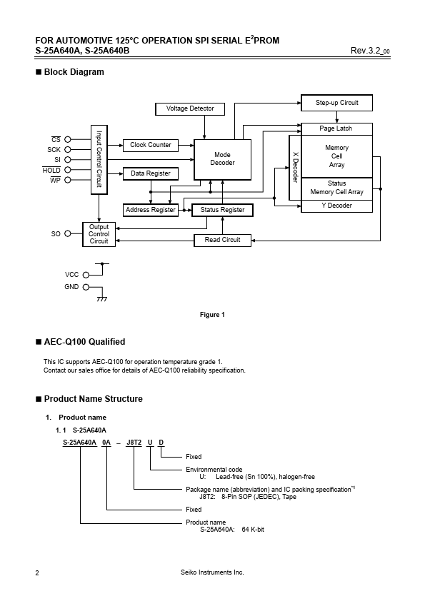
Datasheet Details
| Part number | S-25A640B |
|---|---|
| Manufacturer | Seiko Instruments |
| File Size | 507.36 KB |
| Description | OPERATION SPI SERIAL E2PROM |
| Datasheet |
 S-25A640B Datasheet S-25A640B Datasheet
|
|
|
Download the S-25A640B datasheet PDF. This datasheet also covers the S-25A640A variant, as both devices belong to the same operation spi serial e2prom family and are provided as variant models within a single manufacturer datasheet.
2.
Pin No.
1 SO WP 1 GND SI 1 SCK 1 HOLD 1 VCC Table 4 Description Chip sel
| Part number | S-25A640B |
|---|---|
| Manufacturer | Seiko Instruments |
| File Size | 507.36 KB |
| Description | OPERATION SPI SERIAL E2PROM |
| Datasheet |
S-25A640B Datasheet
|
|
|
|
| Part Number | Description | Manufacturer |
|---|---|---|
| S-25A640B | SPI SERIAL E2PROM | ABLIC |
| S-25A640A | SPI SERIAL E2PROM | ABLIC |
| S-25A010A | SPI SERIAL E2PROM | ABLIC |
| S-25A020A | SPI SERIAL E2PROM | ABLIC |
| S-25A040A | SPI SERIAL E2PROM | ABLIC |
| Part Number | Description |
|---|---|
| S-25A640A | OPERATION SPI SERIAL E2PROM |
| S-25A010A | SPI SERIAL E2PROM |
| S-25A020A | SPI SERIAL E2PROM |
| S-25A040A | SPI SERIAL E2PROM |
| S-25A080A | SPI SERIAL E2PROM |
The following content is an automatically extracted verbatim text from the original manufacturer datasheet and is provided for reference purposes only.