Description
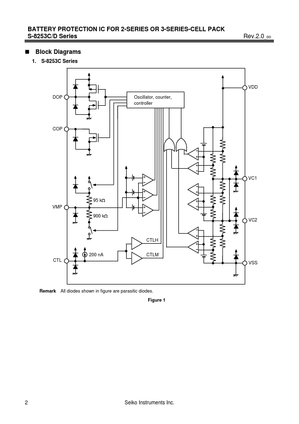
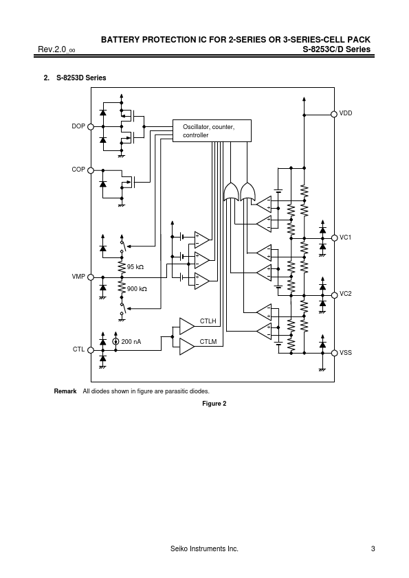
Connection pin for discharge control FET gate
1
DOP
(CMOS output)
2
COP
Connection pin for charge control FET gate (Nch open-drain output)
3
VMP
Pin for voltage detection between VDD and VMP (Detection pin for overcurrent)
Input pin for charge / discharge control signal,
Pin for shortening test time
4 CTL ( L : Normal operation,
H : inhibit charge / discharge
M (VDD × 1 / 2) : shorten test time)
5
VSS
Input pin for negative power supply,
Connection pin for negative voltage of
Features
- (1) High-accuracy voltage detection for each cell.
- Overcharge detection voltage n (n = 1 to 3).
- Overcharge release voltage n (n = 1 to 3)
3.9 V to 4.4 V (50 mV step) 3.8 V to 4.4 V.
- 1
Accuracy ±25 mV Accuracy ±50 mV.
- Overdischarge detection voltage n (n = 1 to 3).
- Overdischarge release voltage n (n = 1 to 3)
2.0 V to 3.0 V (100 mV step) 2.0 V to 3.4 V.
- 2
Accuracy ±80 mV Accuracy ±100 mV
(2) Three-level overcurrent detection (Including load sho.


