K1840
Features
- Largeyfs.
- Enhancement type.
- Low ON resistance.
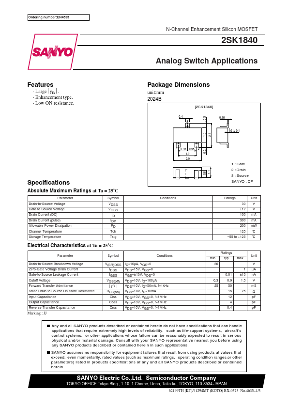
Package Dimensions unit:mm 2024B
[2SK1840]
0.4 3
0 to 0.1
0.5 1.5 0.5 2.5
1 0.95 0.95 2 1.9 2.9
Specifications
Absolute Maximum Ratings at Ta = 25˚C
Parameter Drain-to-Source Voltage Gate-to-Source Voltage Drain Current (DC) Drain Current (pulse) Allowable Power Dissipation Channel Temperature Storage Temperature
Symbol
VDSS VGSS
ID IDP PD Tch
Tstg
Electrical Characteristics at Ta = 25˚C
Conditions
Parameter
Drain-to-Source Breakdown Voltage Zero-Gate Votlage Drain Current Gate-to-Source Leakage Current Cutoff Voltage Forward Transfer Admittance Static Drain-to-Source On-State Resistance Input Capacitance Output Capacitance Reverse Transfer Capacitance Marking : JJ
Symbol
Conditions
V(BR)DSS IDSS IGSS
VGS(off) | yfs |
RDS(on) Ciss
Coss
Crss
ID=10µA, VGS=0 VDS=15V, VGS=0 VGS=±10V, VDS=0 VDS=10V, ID=100µA VDS=10V, ID=50m A, f=1k Hz VGS=10V, ID=10m A VDS=10V, VGS=0, f=1MHz VDS=10V, VGS=0, f=1MHz VDS=10V,...