Description
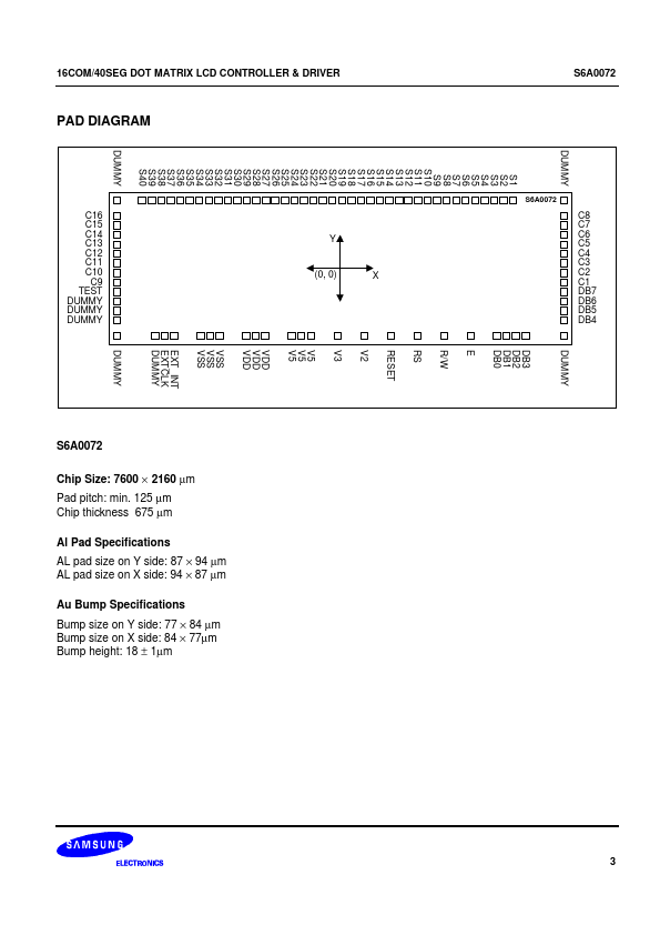
Pin VDD VSS (GND) V2, V3, V5 S1 - S40 C1 - C16 EXTCLK Output Input Input Segment output Common output External clock Input External/internal oscillator clock select Register select Input/Output Power Name Power supply & LCD bias pin Description for logical circuit (+3V, +5V) 0V (GND) Bias voltage level for LCD driving Segment signal output for LCD driving Common signal output for LCD driving When using external clock, used as clock input pin.
Features
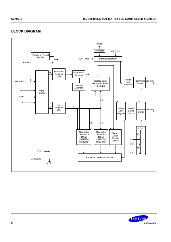
- Internal Memory - Character Generator ROM (CGROM): 9600 bits (240 characters × 5 × 8 dot) - Character Generator RAM (CGRAM): 160 bits (4 characters × 5 × 8 dot) - Display Data RAM (DDRAM): 128 bits (16 characters × 8bits) Low power operation - Power supply voltage range: 2.7 to 5.5V (VDD) - LCD drive voltage range: 3.0 to 11.0 (VDD-V5) CMOS process Duty cycle: 1/16 Built-in oscillator Low power consumption Internal divide resistor for LCD driving voltage COG available.
 S6A0072_Samsungsemiconductor.pdf