Datasheet4U Logo Datasheet4U.com

CD4006 - CMOS 18-Stage Static Register

Description

of “B” Series CMOS Devices” CD4006BM TOP VIEW D1 1 D1 + 4’ 2 CLOCK 3 D2 4 D3 5 D4 6 VSS 7 14 VDD 13 D1 + 4 12 D2 + 5 11 D2 + 4 10 D3 + 4 9 D4 + 5 8 D4 + 4 Functional Diagram VDD 14 Applications Serial Shift Registers Frequency Division Time Delay Circuits Descrip

Features

  • Pinout.
  • High-Voltage Type (20V Rating).
  • Fully Static Operation.
  • Shifting Rates Up to 12MHz at 10V (typ).
  • Permanent Register Storage with Clock Line High or Low - No Information Recirculation Required.
  • 100% Tested for Quiescent Current at 20V.
  • Standardized, Symmetrical Output Characteristics.
  • 5V, 10V and 15V Parametric Ratings.
  • Maximum Input Current of 1µA at 18V Over Full Pack- age-Temperature Range; 100nA at 18V and +25oC.

📥 Download Datasheet

Datasheet Details

Part number CD4006
Manufacturer SYC
File Size 91.99 KB
Description CMOS 18-Stage Static Register
Datasheet download datasheet CD4006 Datasheet

Full PDF Text Transcription

Click to expand full text
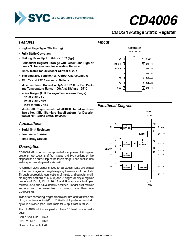
CD4006 CMOS 18-Stage Static Register Features Pinout • High-Voltage Type (20V Rating) • Fully Static Operation • Shifting Rates Up to 12MHz at 10V (typ) • Permanent Register Storage with Clock Line High or Low - No Information Recirculation Required • 100% Tested for Quiescent Current at 20V • Standardized, Symmetrical Output Characteristics • 5V, 10V and 15V Parametric Ratings • Maximum Input Current of 1µA at 18V Over Full Pack- age-Temperature Range; 100nA at 18V and +25oC • Noise Margin (Full Package-Temperature Range): - 1V at VDD = 5V - 2V at VDD = 10V - 2.5V at VDD = 15V • Meets All Requirements of JEDEC Tentative Standards No.
Published: |