Datasheet Details
| Part number | W25NM60N |
|---|---|
| Manufacturer | STMicroelectronics |
| File Size | 548.83 KB |
| Description | STW25NM60N |
| Datasheet |
 W25NM60N Datasheet W25NM60N Datasheet
|
|
|
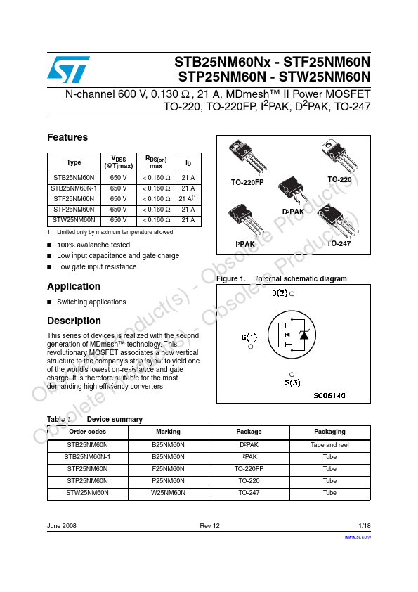
du - OThis series of devices is realized with the second ro )generation of MDmesh™ technology.
This P t(srevolutionary MOSFET associates a new vertical te cstructure to the company’s strip layout to yield one le uof the world’s lowest on-resistance and gate dcharge.
| Part number | W25NM60N |
|---|---|
| Manufacturer | STMicroelectronics |
| File Size | 548.83 KB |
| Description | STW25NM60N |
| Datasheet |
W25NM60N Datasheet
|
|
|
|