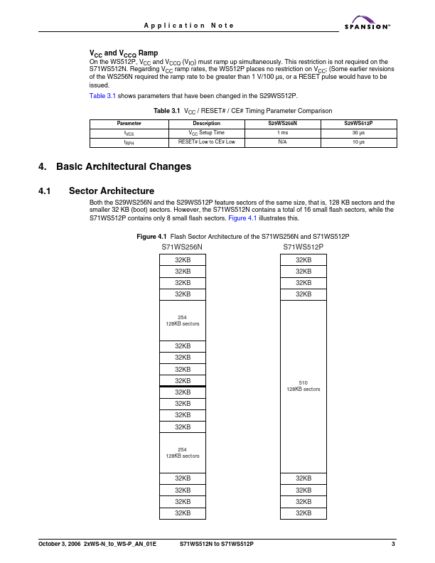
Description
- Package and Pin Layout
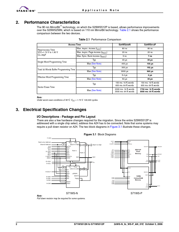
There are also a few hardware changes required for the migration.Since the entire S29WS512P is addressed with a single chip select, address line A24 has to be connected.Note that some systems may require a pull down resistor on A24. The two block diagrams in Figure 3.1 illustrate these changes.Figure 3.1 Block Diagrams
F-VCC Flash-only Address Shared Address CLK WP# ACC F1-CE# OE# WE# F-RST# AVD# F2-CE# R-VCC 22 VCC CLK CE# WE# OE# UB# LB# VCCQ 16 VID DQ15 to DQ0 CLK
Features
- between the two flash device cores. Table 1.1 Comparison of Key Features
Futures Technology Process Rule VCC VIO (VCCQ) Max Density Configuration Register Sector Architecture Bank Architecture Bank Size Boot Option Common Flash Interface (CFI) Simultaneous Read/Write Asynchronous Read Mode Page Mode Read Page Size Synchronous (Burst) Read Mode Burst Frequency Burst Length Single Word / Write Buffer Program Write Buffer Size Program Suspend / Program Resume Sector Erase / Chip Erase Erase Suspend.
 S29WS512P_SPANSION.pdf