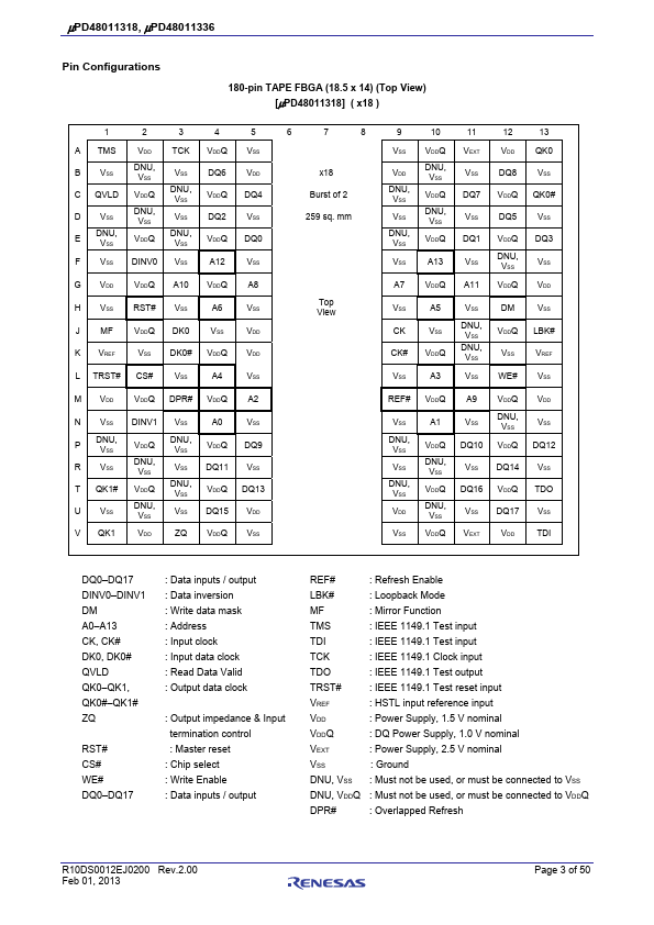
Download the UPD48011336 datasheet PDF.
This datasheet also covers the UPD48011318 variant, as both devices belong to the same low latency dram family and are provided as variant models within a single manufacturer datasheet.
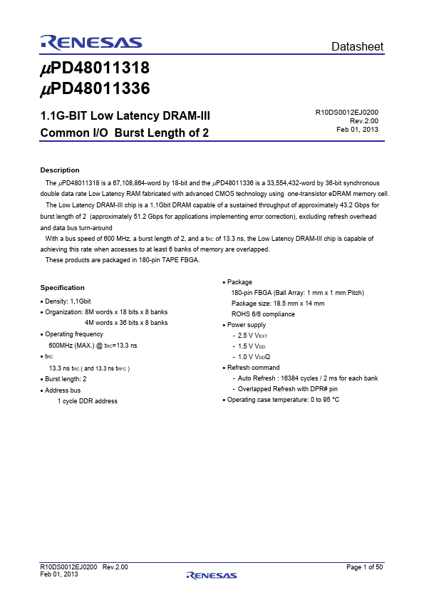
Description
double data rate Low Latency RAM fabricated with advanced CMOS technology using one-transistor eDRAM memory cell.
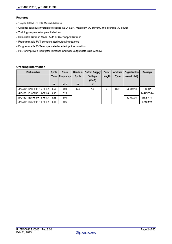
Features
- 1 cycle 600MHz DDR Muxed Address.
- Optional data bus inversion to reduce SSO, SSN, maximum I/O current, and average I/O power.
- Training sequence for per-bit deskew.
- Selectable Refresh Mode: Auto or Overlapped Refresh.
- Programmable PVT-compensated output impedance.
- Programmable PVT-compensated on-die input termination.
- PLL for improved input jitter tolerance and wide output data valid window
Ordering Information
Part number
Cycle C.
 UPD48011336 Datasheet