Description
FIXED (5.0V, 3.3V, 3.0V) PIN NUMBER
1
ADJUSTABLE OUTPUT PIN NUMBER
1
2
2
3
3
4
-
-
4
5
5
6
6
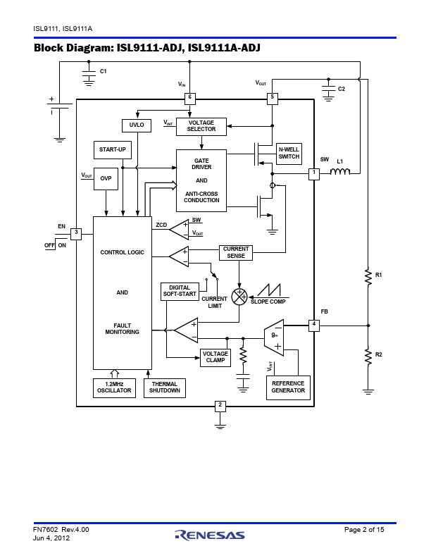
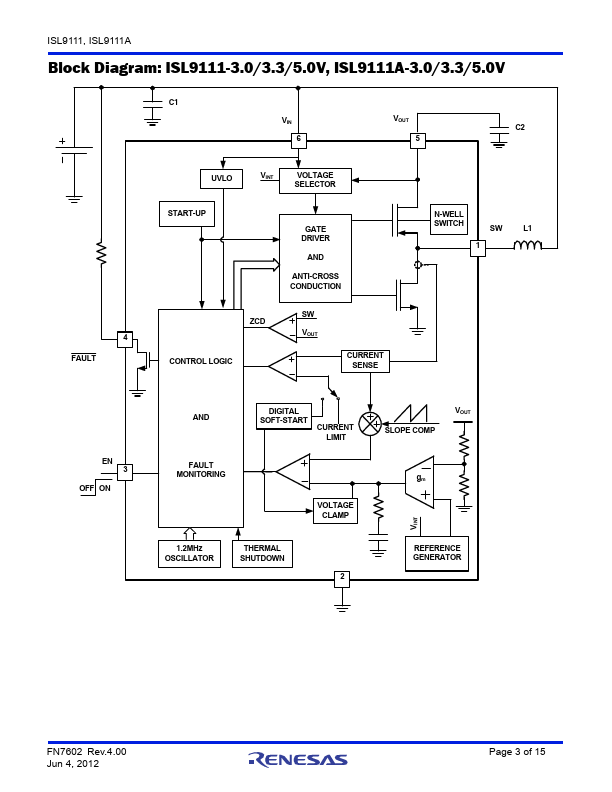
SYMBOL SW GND EN
FAULT FB
VOUT VIN
PIN DESCRIPTION
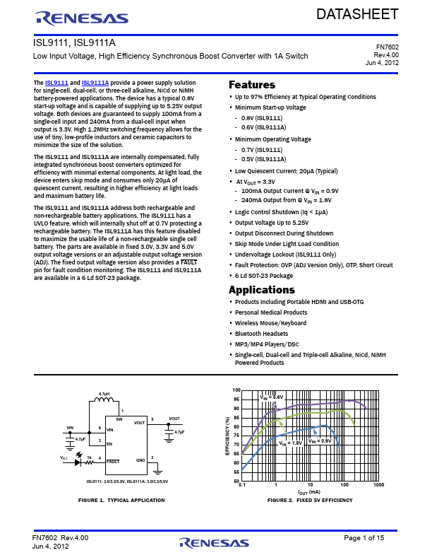
The SW pin is the switching node of the power converter.Connect one terminal of the inductor to the SW pin and the other to power input.System ground
The EN pin is an active-high logic input for enabling the device.When asserted high, the boost function begins.When asserted low, the device is completely disabled, and current is block
Features
- Up to 97% Efficiency at Typical Operating Conditions.
- Minimum Start-up Voltage
- 0.8V (ISL9111) - 0.6V (ISL9111A).
- Minimum Operating Voltage - 0.7V (ISL9111) - 0.5V (ISL9111A).
- Low Quiescent Current: 20μA (Typical).
- At VOUT = 3.3V
- 100mA Output Current @ VIN = 0.9V - 240mA Output from @ VIN = 1.8V.
- Logic Control Shutdown (Iq < 1µA).
- Output Voltage Up to 5.25V.
- Output Disconnect During Shutdown.
- Skip Mode Under Lig.
 ISL9111-Renesas.pdf