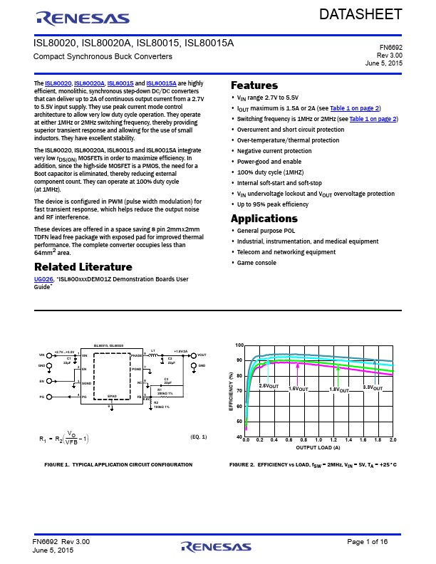
Description
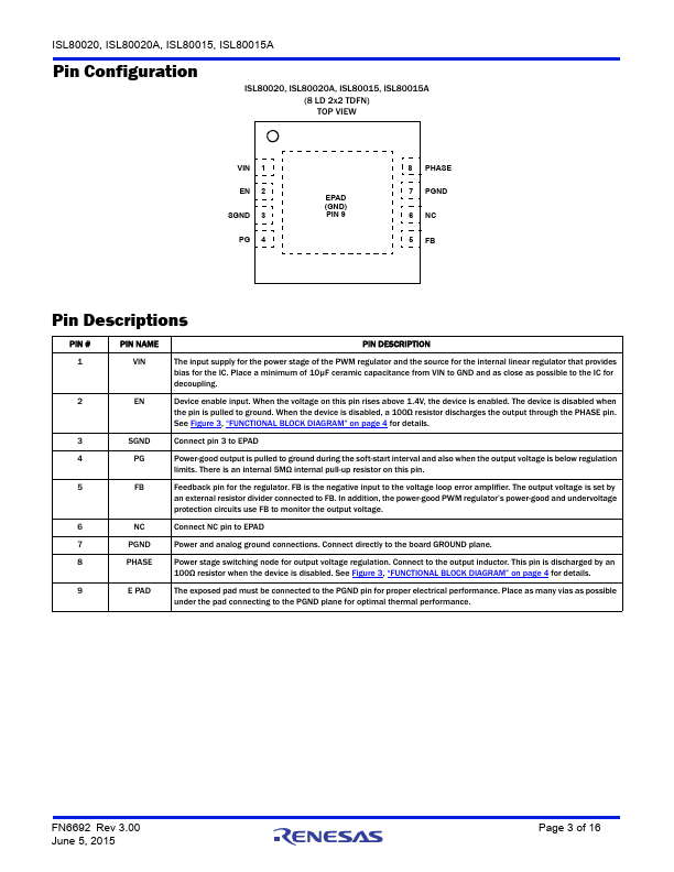
PIN # 1
2
3 4 5
6 7 8 9
PIN NAME VIN
EN
SGND PG FB
NC PGND PHASE E PAD
PIN DESCRIPTION
The input supply for the power stage of the PWM regulator and the source for the internal linear regulator that provides bias for the IC.Place a minimum of 10µF ceramic capacitance from VIN to GND and as close as possible to the IC for decoupling.Device enable input.When the voltage on this pin rises above 1.4V, the device is enabled.The device is disabled when the pin is pulled to ground.When the dev
Features
- VIN range 2.7V to 5.5V.
- IOUT maximum is 1.5A or 2A (see Table 1 on page 2).
- Switching frequency is 1MHz or 2MHz (see Table 1 on page 2).
- Overcurrent and short circuit protection.
- Over-temperature/thermal protection.
- Negative current protection.
- Power-good and enable.
- 100% duty cycle (1MHZ).
- Internal soft-start and soft-stop.
- VIN undervoltage lockout and VOUT overvoltage protection.
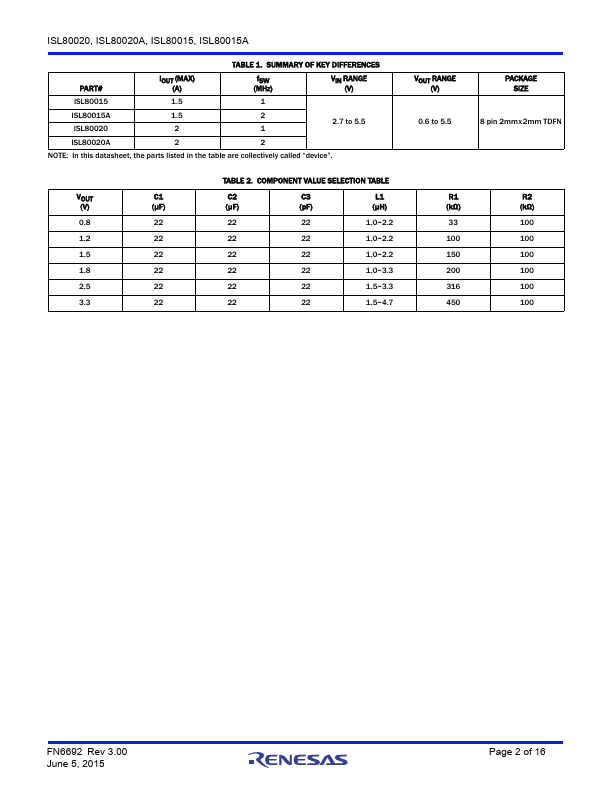
- Up to 95% peak.
 ISL80020-Renesas.pdf