Datasheet Details
| Part number | 87016I |
|---|---|
| Manufacturer | Renesas |
| File Size | 605.84 KB |
| Description | LVCMOS/LVTTL Clock Generator |
| Datasheet |
 87016I Datasheet 87016I Datasheet
|
|
|
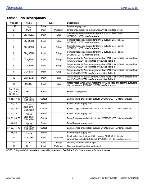
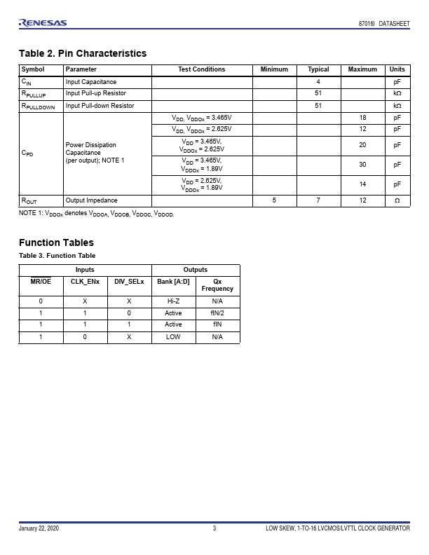
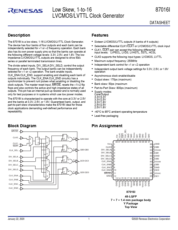
The 87016I is a low skew, 1:16 LVCMOS/LVTTL Clock Generator.
The device has four banks of four outputs and each bank can be independently selected for 1 or 2 frequency operation.
| Part number | 87016I |
|---|---|
| Manufacturer | Renesas |
| File Size | 605.84 KB |
| Description | LVCMOS/LVTTL Clock Generator |
| Datasheet |
87016I Datasheet
|
|
|
|