Datasheet Details
| Part number | MN3890S |
|---|---|
| Manufacturer | Panasonic Semiconductor |
| File Size | 53.10 KB |
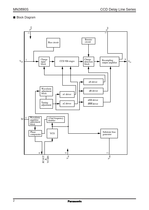
| Description | NTSC-Compatible CCD 1 H Video Signal Delay Element |
| Datasheet |
 MN3890S Datasheet MN3890S Datasheet
|
|
|
| Part number | MN3890S |
|---|---|
| Manufacturer | Panasonic Semiconductor |
| File Size | 53.10 KB |
| Description | NTSC-Compatible CCD 1 H Video Signal Delay Element |
| Datasheet |
MN3890S Datasheet
|
|
|
|
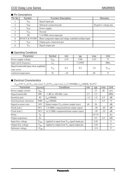
Pin No.
📁 Similar Datasheet