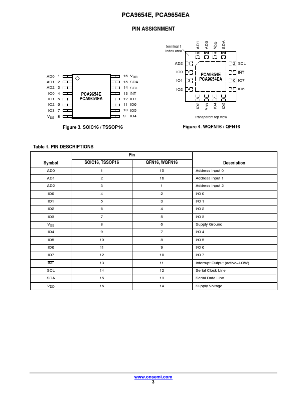
Description
Symbol AD0 AD1 AD2 IO0 IO1 IO2 IO3 VSS IO4 IO5 IO6 IO7 INT SCL SDA VDD
SOIC16, TSSOP16 1 2 3 4 5 6 7 8 9 10 11 12 13 14 15 16
Pin
QFN16, WQFN16 15 16 1 2 3 4 5 6 7 8 9 10 11 12 13 14
Description Address Input 0 Address Input 1 Address Input 2 I/O 0 I/O 1 I/O 2 I/O 3 Supply Ground I/O 4 I/O 5 I/O 6 I/O 7 Interrupt Output (active
LOW) Serial Clock Line Serial Data Line Supply Voltage
www.onsemi.com 3
PCA9654E, PCA9654EA
Table 2. MAXIMUM RATINGS
Symbol
Parameter
Value
Unit
VDD
Features
- VDD Operating Range: 1.65 V to 5.5 V.
- SDA Sink Capability: 30 mA.
- 5.5 V Tolerant I/Os.
- Polarity Inversion Register.
- Active LOW Interrupt Output.
- Low Standby Current.
- Noise Filter on SCL/SDA Inputs.
- No Glitch on Power.
- up.
- Internal Power.
- on Reset.
- 64 Programmable Slave Addresses Using 3 Address Pins.
- 8 I/O Pins which Default to 8 Inputs.
- I2C SCL Clock Frequencies Supported:.
 PCA9654E-ONSemiconductor.pdf