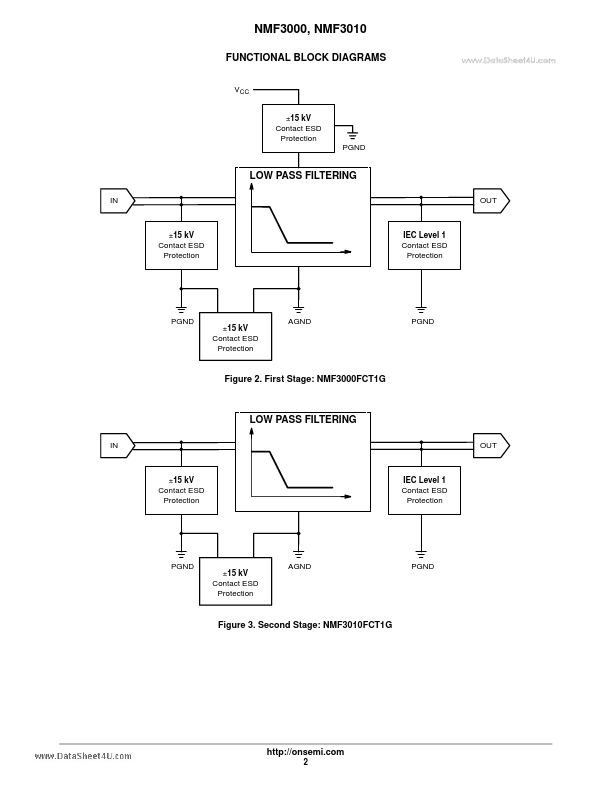
Description
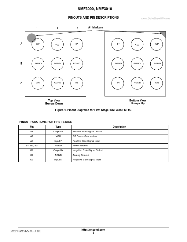
A1 Markers
www.DataSheet4U.com
1
2
3
A
OP
Vcc
IP
IP
Vcc
OP
B
PGND
PGND
PGND
PGND
PGND
PGND
C
ON
AGND
IN
IN
AGND
ON
Top View Bumps Down
Bottom View Bumps Up
Figure 4. Pinout Diagrams for First Stage: NMF3000FCT1G
PINOUT FUNCTIONS FOR FIRST STAGE
Pin A1 A2 A3 B1, B2, B3 C1 C2 C3 Type Output P VCC Input P PGND Output N AGND Input N Positive Side Signal Output DC Power Connection Positive Side Signal Input Power Ground Negative Side Signal Output Analog Ground Negative S
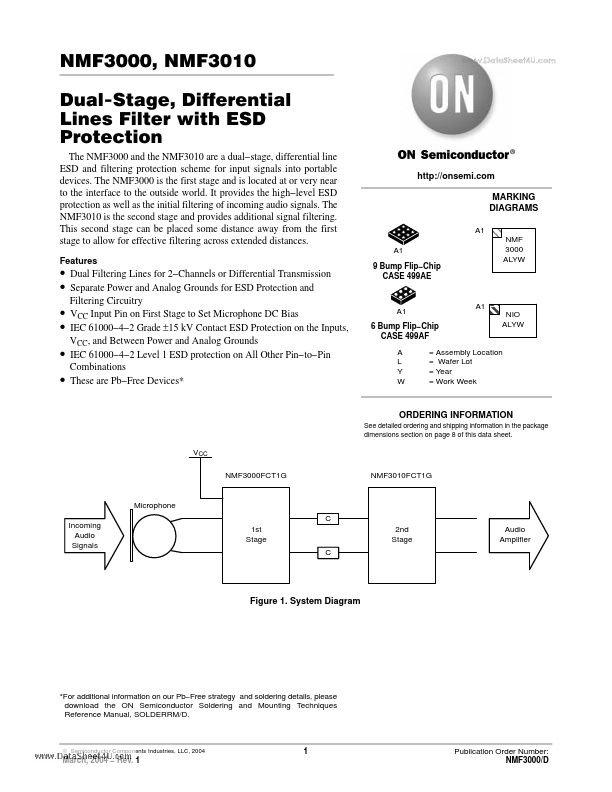
Features
- Dual Filtering Lines for 2.
- Channels or Differential Transmission.
- Separate Power and Analog Grounds for ESD Protection and.
- VCC Input Pin on First Stage to Set Microphone DC Bias.
- IEC 61000.
- 4.
- 2 Grade ±15 kV Contact ESD Protection on the Inputs,.
- IEC 61000.
- 4.
- 2 Level 1 ESD protection on All Other Pin.
- to.
- Pin.
- Combinations These are Pb.
- Free Devices.
- VCC, and Between Power and A.
 NMF3010 Datasheet