Datasheet Details
| Part number | NCP700B |
|---|---|
| Manufacturer | onsemi |
| File Size | 625.33 KB |
| Description | BiCMOS RF LDO Regulator |
| Datasheet |
 NCP700B Datasheet NCP700B Datasheet
|
|
|
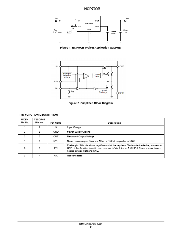
WDFN Pin No.
5 Pin No.
Description Input Voltage Power Supply Ground Regulated Output Voltage Noise reduction pin.
(Connect 10 nF or 100 nF capacitor to GND) Enable pin: This pin allows on/off control of the regulator.
| Part number | NCP700B |
|---|---|
| Manufacturer | onsemi |
| File Size | 625.33 KB |
| Description | BiCMOS RF LDO Regulator |
| Datasheet |
NCP700B Datasheet
|
|
|
|
| Part Number | Description | Manufacturer |
|---|---|---|
| NCP-NFJ | C15 Type Accessories | Hirose Electric |
| NCP-NFP | C15 Type Accessories | Hirose Electric |
| NCP03WB473E05RL | Thermistors | Murata |
| NCP03WB473J05RL | NTC Thermistors | Murata |
| NCP03WB473J05RL | Thermistors | Murata |
| Part Number | Description |
|---|---|
| NCP700 | BiCMOS RF LDO Regulator |
| NCP700C | BiCMOS RF LDO Regulator |
| NCP702 | LDO Linear Voltage Regulator |
| NCP703 | LDO Voltage Regulator |
| NCP705 | LDO Voltage Regulator |
The following content is an automatically extracted verbatim text from the original manufacturer datasheet and is provided for reference purposes only.