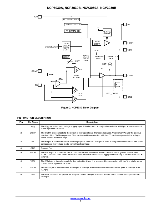
Description
Pin Pin Name
Description
1 VCC The VCC pin is the main voltage supply input.It is also used in conjunction with the VSW pin to sense current in the high side MOSFET.2 COMP The COMP pin connects to the output of the Operational Transconductance Amplifier (OTA) and the positive terminal of the PWM comparator.This pin is used in conjunction with the FB pin to compensate the voltage mode control feedback loop.3 FB The FB pin is connected to the inverting input of the OTA.This pin is used i
Features
- include lossless current limit and short circuit protection, output overvoltage protection, output undervoltage protection, and input undervoltage lockout. The NCP3030 is currently available in a SOIC.
- 8 package. Features.
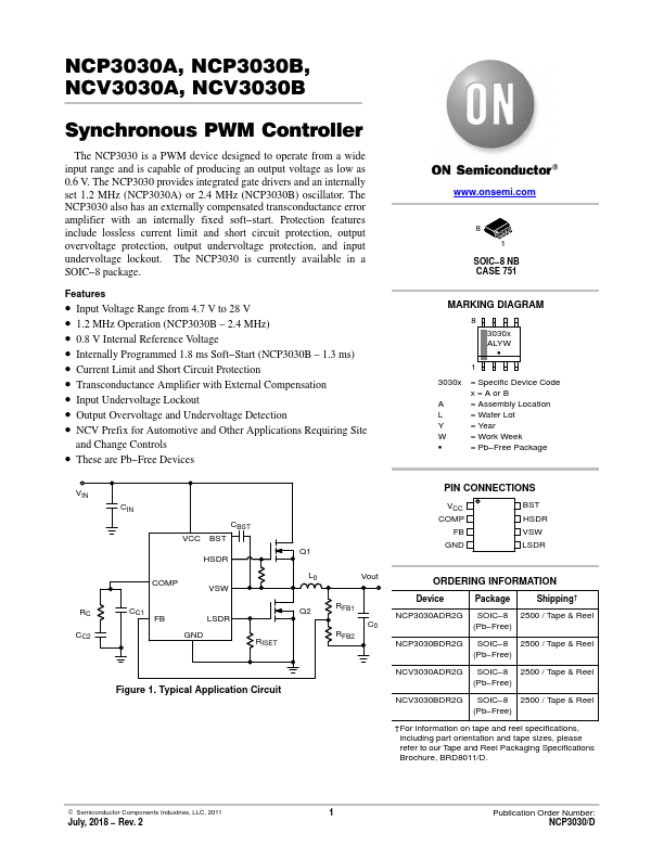
- Input Voltage Range from 4.7 V to 28 V.
- 1.2 MHz Operation (NCP3030B.
- 2.4 MHz).
- 0.8 V Internal Reference Voltage.
- Internally Programmed 1.8 ms Soft.
- Start (NCP3030B.
- 1.3 ms).
- Current Limit and Short Ci.
 NCP3030A-ONSemiconductor.pdf