Datasheet Details
| Part number | NCP1599 |
|---|---|
| Manufacturer | ON Semiconductor ↗ |
| File Size | 534.87 KB |
| Description | 3 A Synchronous Buck Regulator |
| Datasheet |
 NCP1599_ONSemiconductor.pdf NCP1599_ONSemiconductor.pdf
|
| Part number | NCP1599 |
|---|---|
| Manufacturer | ON Semiconductor ↗ |
| File Size | 534.87 KB |
| Description | 3 A Synchronous Buck Regulator |
| Datasheet |
NCP1599_ONSemiconductor.pdf
|
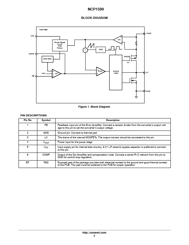
Pin No Symbol 1 FB 2 GND 3 LX 4 VCCP 5 VCC 6 COMP EP PAD Figure 1. Block Diagram Description Feedback input pin of the Error Amplifier.Connect a resistor divider from the converter’s output voltage to this pin to set the converter’s output voltage.Ground pin.Connect to thermal pad.The drains of the internal MOSFETs.The output inductor should be connected to this pin.Power input for the power stage Input supply pin for internal bias circuitry.A 0.1 mF ceramic bypass capacitor is pre
📁 NCP1599 Similar Datasheet