Datasheet4U Logo Datasheet4U.com

NBSG14 - SiGe Differential 1:4 Clock/Data Driver

General Description

MARKING DIAGRAMS The NBSG14 is a 1 to 4 clock/data distribution chip, optimized for ultra

low skew and jitter.

Inputs incorporate internal 50 W termination resistors and accept NECL (Negative ECL), PECL (Positive ECL), LVTTL, LVCMOS, CML, or LVDS.

Key Features

  • SG 14 ALYW FCBGA.
  • 16 BA SUFFIX CASE 489.
  • Maximum Input Clock Frequency up to 12 GHz Typical Maximum Input Data Rate up to 12 Gb/s Typical 30 ps Typical Rise and Fall Times 125 ps Typical Propagation Delay RSPECL Output with Operating Range: VCC = 2.375 V to 3.465 V with VEE = 0 V RSNECL Output with RSNECL or NECL Inputs with Operating Range: VCC = 0 V with VEE =.
  • 2.375 V to.

📥 Download Datasheet

Datasheet Details

Part number NBSG14
Manufacturer onsemi
File Size 416.46 KB
Description SiGe Differential 1:4 Clock/Data Driver
Datasheet download datasheet NBSG14 Datasheet

Full PDF Text Transcription (Reference)

The following content is an automatically extracted verbatim text from the original manufacturer datasheet and is provided for reference purposes only.

View original datasheet text
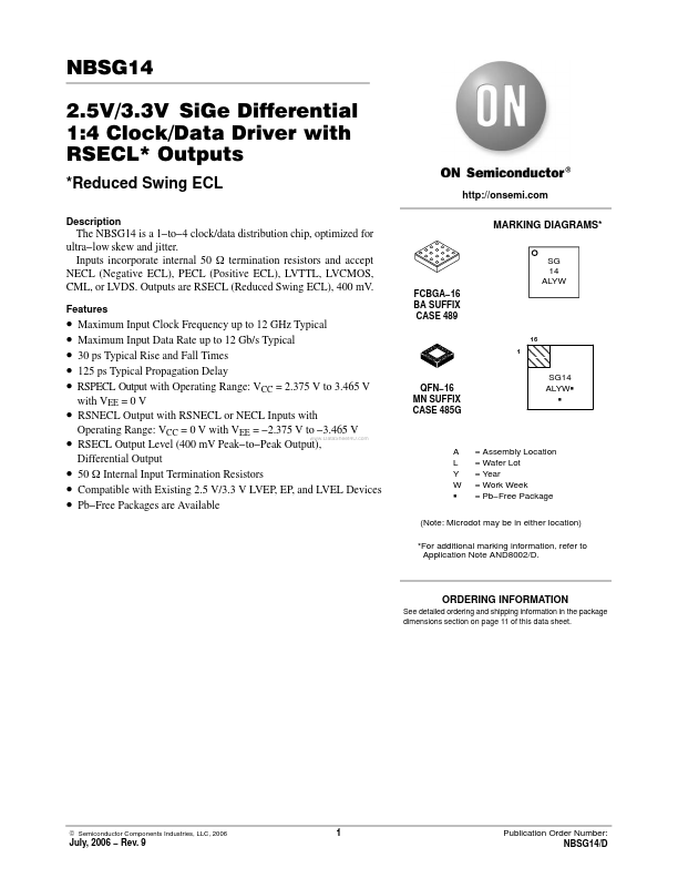
NBSG14 2.5V/3.3V SiGe Differential 1:4 Clock/Data Driver with RSECL* Outputs *Reduced Swing ECL http://onsemi.com Description MARKING DIAGRAMS* The NBSG14 is a 1−to−4 clock/data distribution chip, optimized for ultra−low skew and jitter. Inputs incorporate internal 50 W termination resistors and accept NECL (Negative ECL), PECL (Positive ECL), LVTTL, LVCMOS, CML, or LVDS. Outputs are RSECL (Reduced Swing ECL), 400 mV. Features SG 14 ALYW FCBGA−16 BA SUFFIX CASE 489 • • • • • • • • • • Maximum Input Clock Frequency up to 12 GHz Typical Maximum Input Data Rate up to 12 Gb/s Typical 30 ps Typical Rise and Fall Times 125 ps Typical Propagation Delay RSPECL Output with Operating Range: VCC = 2.375 V to 3.