The following content is an automatically extracted verbatim text
from the original manufacturer datasheet and is provided for reference purposes only.
View original datasheet text
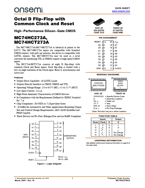
DATA SHEET www.onsemi.com
Octal D Flip-Flop with Common Clock and Reset
High−Performance Silicon−Gate CMOS
MC74HC273A, MC74HCT273A
The MC74HC273A/MC74HCT273A is identical in pinout to the LS273. The MC74HC273A inputs are compatible with Standard CMOS outputs; with pull−up resistors, the device is compatible with LSTTL outputs. The MC74HCT273A may be used as a level converter for interfacing TTL or NMOS outputs to high speed CMOS inputs.
The HC273A/HCT273A consists of eight D flip−flops with common Clock and Reset inputs. Each flip−flop is loaded with a low−to−high transition of the Clock input. Reset is asynchronous and active low.
Features
• Output Drive Capability: 10 LSTTL Loads • Outputs Directly Interface to CMOS, NMOS and TTL • Operating Voltage Range: 2.0 to 6.0 V (HC), 4.5 to 5.
 MC74HCT273A Datasheet