Datasheet4U Logo Datasheet4U.com

MC74ACT299 Datasheet - ON Semiconductor

MC74ACT299 8-Input Universal Shift/Storage Register

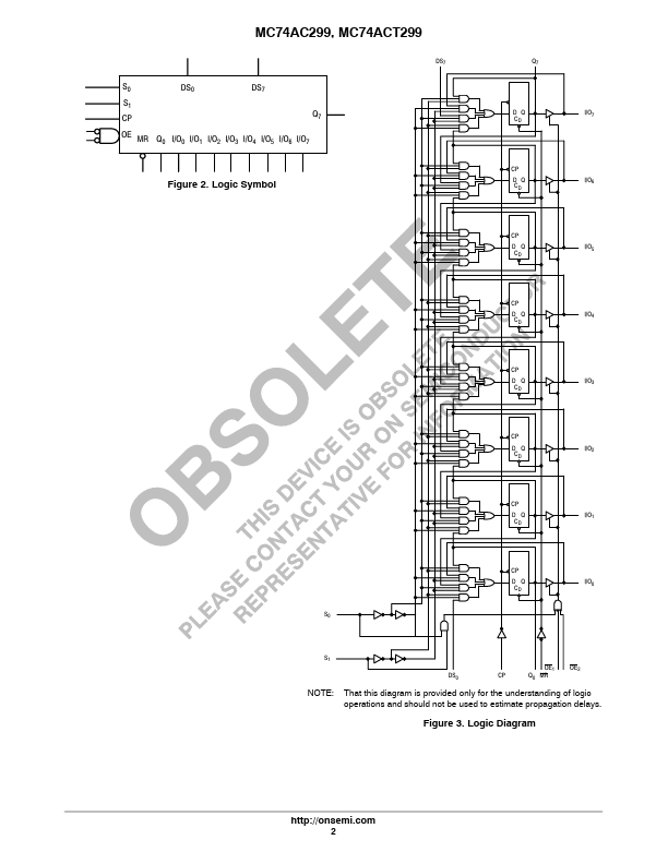
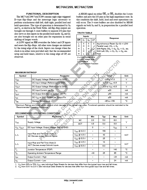
The MC74AC299/74ACT299 contains eight edge *triggered D *type flip *flops and the interstage logic necessary to perform synchronous shift left, shift right, parallel load and hold operations. The type of operation is determined by S0 and S1, as shown in the Truth Table. All flip.
MC74AC299, MC74ACT299 8 Input Universal Shift/ Storage Register with Common Parallel I/O Pins The MC74AC299/74ACT299 is an 8 bit universal shift/storage register with 3 state outputs. Four modes of operation are possible: hold (store), shift left, shift right and load data. The parallel load inputs and flip flop outputs are multiplexed to reduce the total number of package pins. Additional outputs are provided for flip flops Q0, Q7 to allow easy serial ca.

MC74ACT299 Datasheet (254.48 KB)

Preview of MC74ACT299 PDF
MC74ACT299 Datasheet Preview Page 2 MC74ACT299 Datasheet Preview Page 3

Datasheet Details

Part number:

MC74ACT299

Manufacturer:

ON Semiconductor ↗

File Size:

254.48 KB

Description:

8-input universal shift/storage register.

📁 Related Datasheet

MC74ACT299 8-Input Universal Shift/Storage Register (Motorola)

MC74ACT20 Dual 4-Input NAND Gate (ON Semiconductor)

MC74ACT20 DUAL 4-INPUT NAND GATE (Motorola)

MC74ACT240 Octal Buffer/Line Driver (ON Semiconductor)

MC74ACT240 OCTAL BUFFER/LINE DRIVER (Motorola)

MC74ACT241 Octal Buffer/Line Driver (ON Semiconductor)

MC74ACT241 OCTAL BUFFER/LINE DRIVER (Motorola)

MC74ACT244 Octal Buffer/Line Driver (ON Semiconductor)

TAGS

MC74ACT299 8-Input Universal Shift Storage Register ON Semiconductor

MC74ACT299 Distributor