Datasheet Details
| Part number | FDD5690 |
|---|---|
| Manufacturer | ON Semiconductor |
| File Size | 234.91 KB |
| Description | N-Channel MOSFET |
| Datasheet |
 FDD5690 Datasheet FDD5690 Datasheet
|
|
|
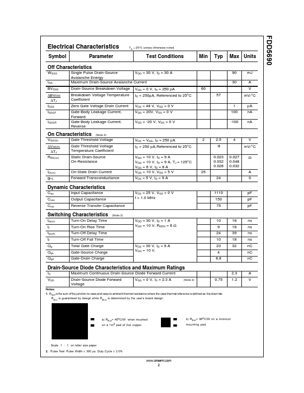
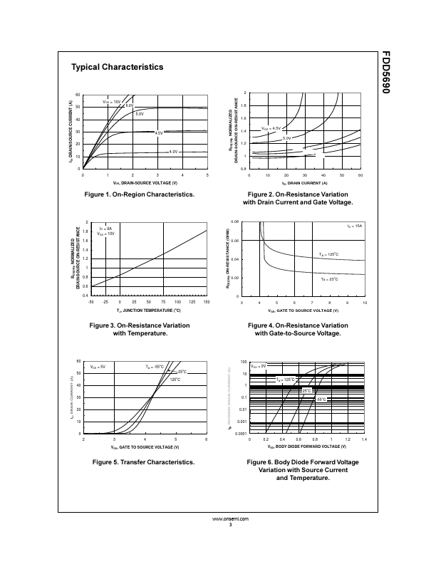
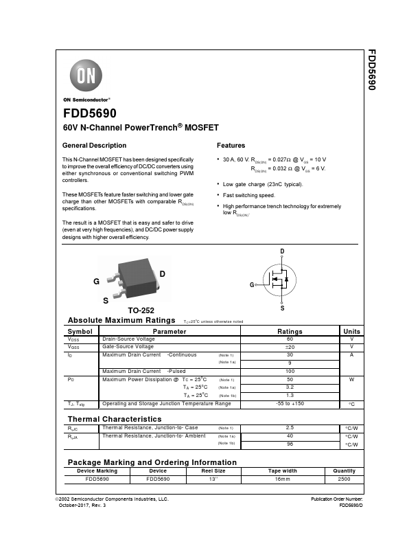
This N-Channel MOSFET has been designed specifically to improve the overall efficiency of DC/DC converters using either synchronous or conventional switching PWM controllers.
These MOSFETs feature faster switching and lower gate charge than other MOSFETs with comparable RDS(ON) specifications.
| Part number | FDD5690 |
|---|---|
| Manufacturer | ON Semiconductor |
| File Size | 234.91 KB |
| Description | N-Channel MOSFET |
| Datasheet |
FDD5690 Datasheet
|
|
|
|