Datasheet Details
- Part number
- 25FU406C
- Manufacturer
- ON Semiconductor ↗
- File Size
- 166.83 KB
- Datasheet
- 25FU406C-ONSemiconductor.pdf
- Description
- SPI bus flash memory
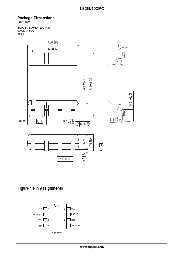
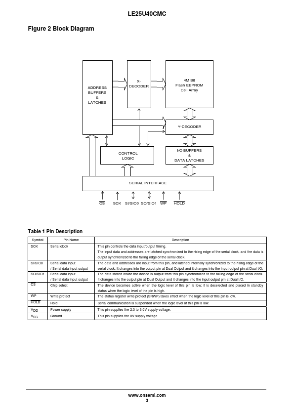
Symbol SCK Pin Name Serial clock SI/SIO0 SO/SIO1 CS Serial data input / Serial data input output Serial data input / Serial data input output Chip select WP HOLD VDD VSS Write protect Hold Power supply Ground Description This pin controls the data input/output timing.The input data and addresses are latched synchronized to the rising edge of the serial clock, and the data is output synchronized to the falling edge of the serial clock.The data and addresses are input from this pin, and l
📁 Related Datasheet
📌 All Tags
25FU406C Stock/Price