Description
Pin Description Pin No
Symbol
Description
1
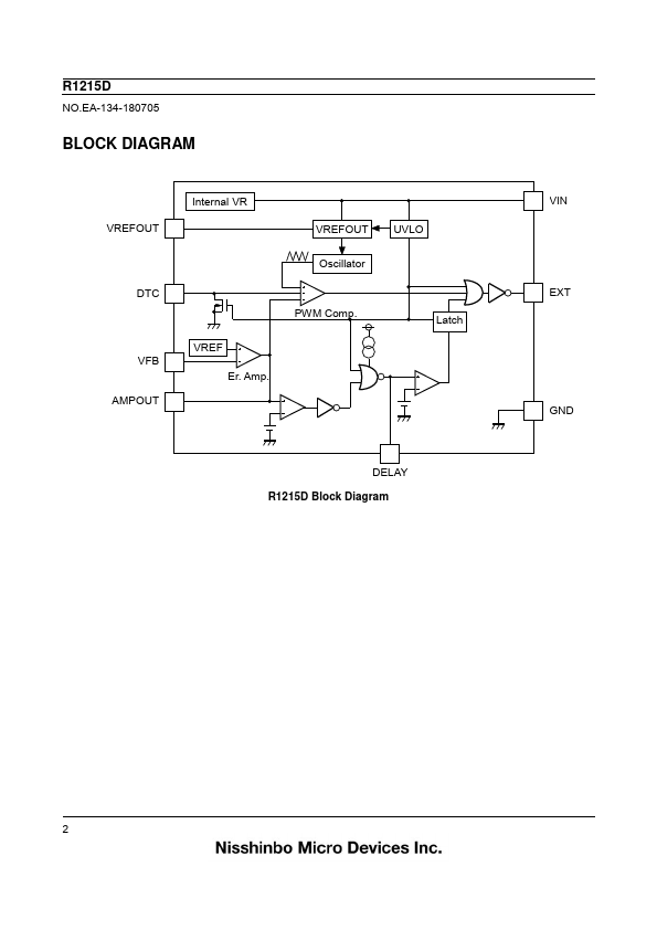
EXT
External FET Drive Pin (CMOS Output)
2
GND
Ground Pin
3
DTC
Pin for Setting Maximum Duty Cycle and Soft start time
4
DELAY
Pin for External Capacitor (for Setting Output Delay of Protection)
5
VFB
Feedback Pin for Monitoring Output Voltage
6
VREFOUT
Reference Voltage Output Pin
7
AMPOUT
Amplifier Output Pin
8
VIN
Power Supply Pin for the IC
∗ Tab suspension leads in the parts have GND level.(They are connected to the re
Features
- Input Voltage Range 1.8 V to 5.5 V.
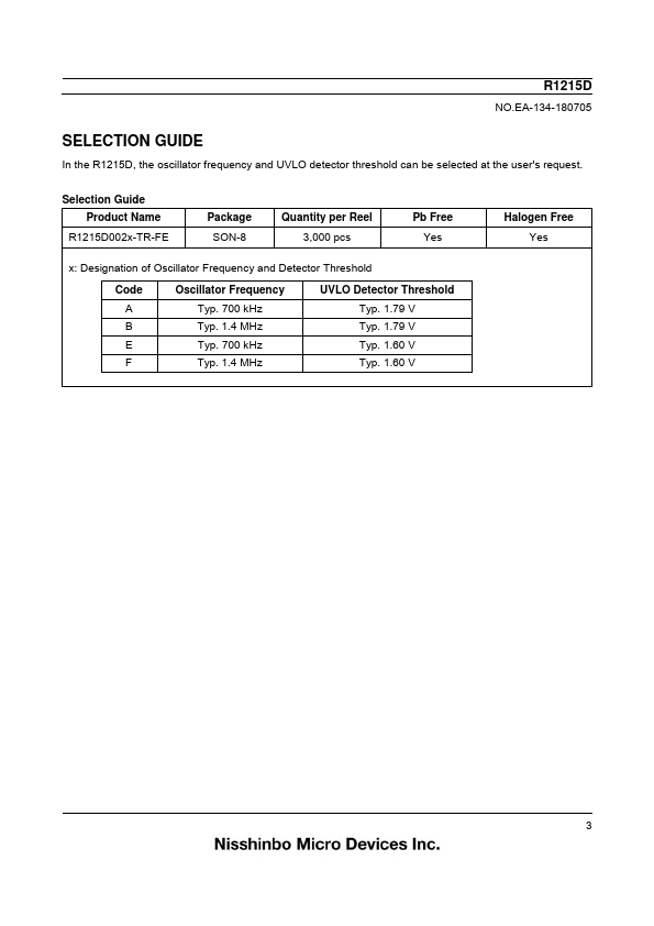
- Two Options of Basic Oscillator Frequency Typ. 700 kHz, 1.4 MHz.
- Built-in Latch-type Protection Function (Output Delay Time can be set with an external capacitor).
- Maximum Duty Cycle/Soft-start time Adjustable with external capacitors.
- High Reference Voltage Accuracy ±1.5%.
- UVLO Threshold level Typ. 1.6 V/ 1.79 V by mask option.
- Small Temperature Coefficient of Reference Voltage Typ. ±150 pp.
 R1215D-Nisshinbo.pdf