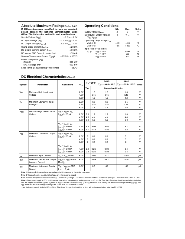
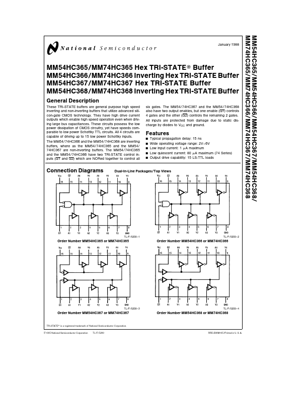
These TRI-STATE buffers are general purpose high speed inverting and non-inverting buffers that utilize advanced silicon-gate CMOS technology They have high drive current outputs which enable high speed operation even when driving large bus capacitances These circuits possess the low power dissipati
Features
Y Y Y Y Y
Typical propagation delay 15 ns Wide operating voltage range 2V.
6V Low input current 1 mA maximum Low quiescent current 80 mA maximum (74 Series) Output drive capability 15 LS-TTL loads
Connection Diagrams
Dual-In-Line Packages Top Views
TL F 5209.
1
TL F 5209.
2
Order Number MM54HC365 or MM74HC365
Order Number MM54HC366 or MM74HC366
TL F 5209.
3
TL F 5209.
4
Order Number MM54HC367 or MM74HC367
Order Number MM54HC368 or MM74HC368.
The following content is an automatically extracted verbatim text
from the original manufacturer datasheet and is provided for reference purposes only.
View original datasheet text
MM54HC365 MM54HC366 MM54HC367 MM54HC368 MM74HC365 MM74HC366 MM74HC367 MM74HC368
January 1988
MM54HC365 MM54HC366 MM54HC367 MM54HC368
MM74HC365 Hex TRI-STATE Buffer MM74HC366 Inverting Hex TRI-STATE Buffer MM74HC367 Hex TRI-STATE Buffer MM74HC368 Inverting Hex TRI-STATE Buffer
six gates The MM54 74HC367 and the MM54 74HC368 also have two output enables but one enable (G1) controls 4 gates and the other (G2) controls the remaining 2 gates All inputs are protected from damage due to static discharge by diodes to VCC and ground
General Description
These TRI-STATE buffers are general purpose high speed inverting and non-inverting buffers that utilize advanced silicon-gate CMOS technology They have high drive current outputs which enable high speed operation even when driving large bus capac
 MM54HC366 Datasheet