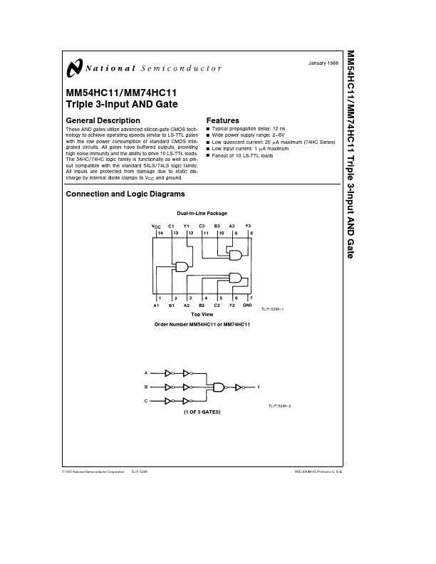
These AND gates utilize advanced silicon-gate CMOS technology to achieve operating speeds similar to LS-TTL gates with the low power consumption of standard CMOS integrated circuits All gates have buffered outputs providing high noise immunity and the ability to drive 10 LS-TTL loads The 54HC 74HC l
Features
Y Y Y Y Y
Typical propagation delay 12 ns Wide power supply range 2.
6V Low quiescent current 20 mA maximum (74HC Series) Low input current 1 mA maximum Fanout of 10 LS-TTL loads
Connection and Logic Diagrams
Dual-In-Line Package
TL F 5298.
1
Top View Order Number MM54HC11 or MM74HC11
TL F 5298.
2
(1 OF 3 GATES)
C1995 National Semiconductor Corporation
TL F 5298
RRD-B30M105 Printed in U S A
Absolute Maximum Ratings (Notes 1
2)
Operating Conditions
Supply Vo.
The following content is an automatically extracted verbatim text
from the original manufacturer datasheet and is provided for reference purposes only.
View original datasheet text
MM54HC11 MM74HC11 Triple 3-Input AND Gate
January 1988
MM54HC11 MM74HC11 Triple 3-Input AND Gate
General Description
These AND gates utilize advanced silicon-gate CMOS technology to achieve operating speeds similar to LS-TTL gates with the low power consumption of standard CMOS integrated circuits All gates have buffered outputs providing high noise immunity and the ability to drive 10 LS-TTL loads The 54HC 74HC logic family is functionally as well as pinout compatible with the standard 54LS 74LS logic family All inputs are protected from damage due to static discharge by internal diode clamps to VCC and ground
Features
Y Y Y Y Y
Typical propagation delay 12 ns Wide power supply range 2 – 6V Low quiescent current 20 mA maximum (74HC Series) Low input current 1 mA maximum Fanout of 10 L
 MM54HC11 Datasheet