Description
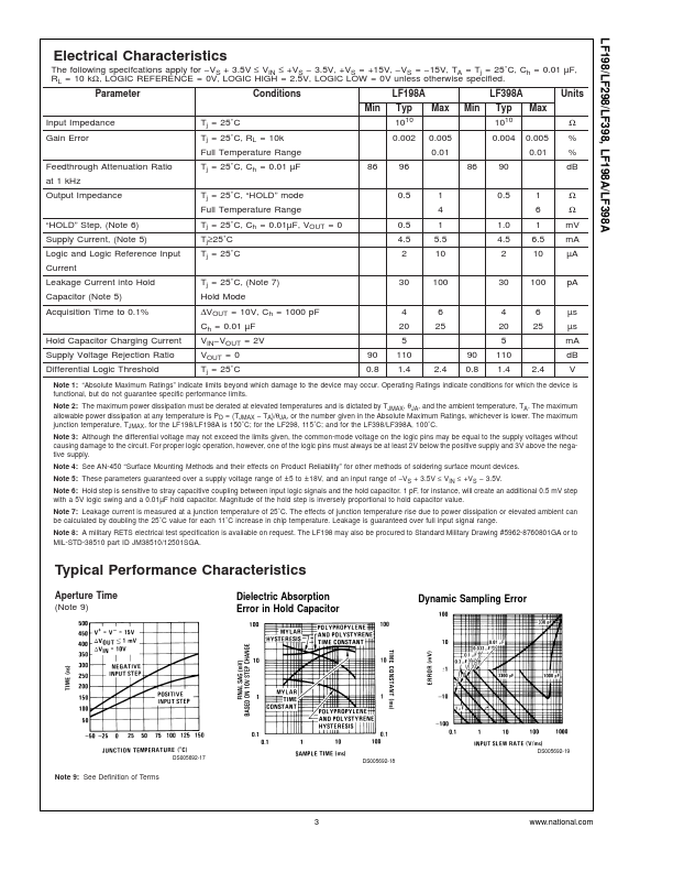
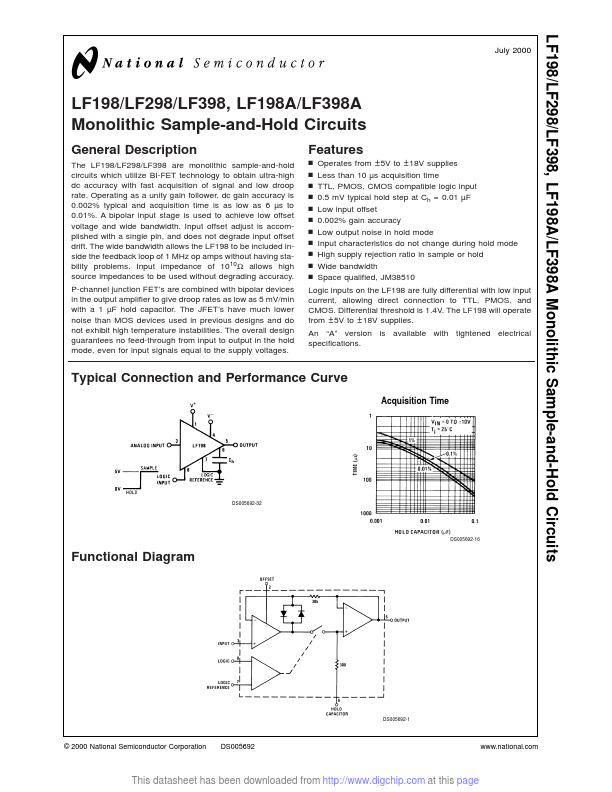
The LF198/LF298/LF398 are monolithic sample-and-hold circuits which utilize BI-FET technology to obtain ultra-high dc accuracy with fast acquisition of signal and low droop rate.
Operating as a unity gain follower, dc gain accuracy is 0.002% typical and acquisition time is as low as 6 µs to 0.01%.
Features
- n Operates from ±5V to ±18V supplies n Less than 10 µs acquisition time n TTL, PMOS, CMOS compatible logic input n 0.5 mV typical hold step at Ch = 0.01 µF n Low input offset n 0.002% gain accuracy n Low output noise in hold mode n Input characteristics do not change during hold mode n High supply rejection ratio in sample or hold n Wide bandwidth n Space qualified, JM38510
Logic inputs on the LF198 are fully differential with low input current, allowing direct connection to TTL, PMOS, and CMOS.
 LF198A Datasheet