Datasheet Details
| Part number | DS90LV001 |
|---|---|
| Manufacturer | National Semiconductor (Texas Instruments) |
| File Size | 396.43 KB |
| Description | 3.3V LVDS-LVDS Buffer |
| Datasheet |
 DS90LV001 Datasheet DS90LV001 Datasheet
|
|
|
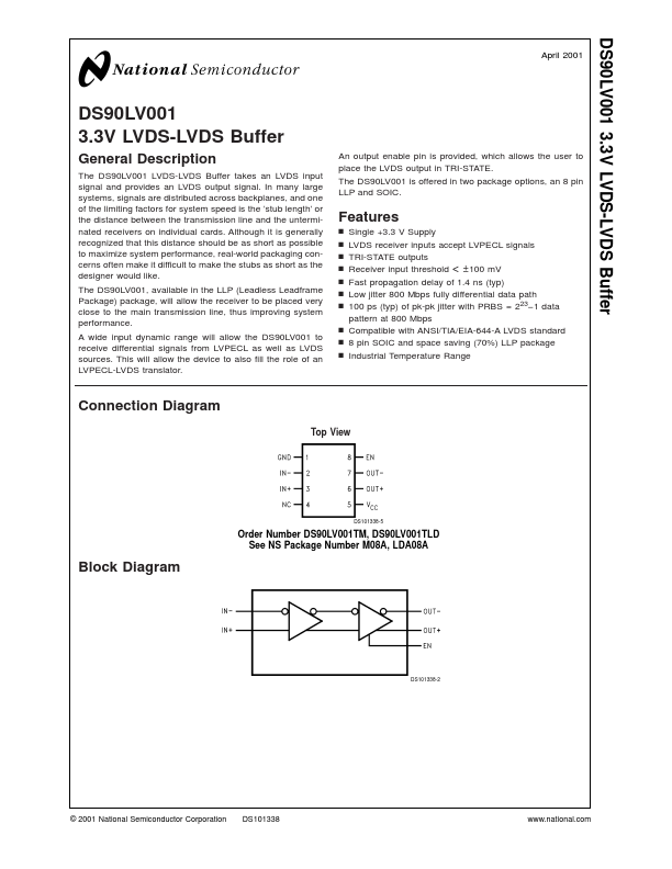
The DS90LV001 LVDS-LVDS Buffer takes an LVDS input signal and provides an LVDS output signal.
| Part number | DS90LV001 |
|---|---|
| Manufacturer | National Semiconductor (Texas Instruments) |
| File Size | 396.43 KB |
| Description | 3.3V LVDS-LVDS Buffer |
| Datasheet |
DS90LV001 Datasheet
|
|
|
|
| Part Number | Description | Manufacturer |
|---|---|---|
| DS90LV001 | 800-Mbps LVDS Buffer | Texas Instruments |
| DS90LV004 | 4-Channel LVDS Buffer/Repeater | Texas Instruments |
| DS90LV011A | 3V LVDS Single High Speed Differential Driver | Texas Instruments |
| DS90LV011AH | High Temperature 3-V LVDS Differential Driver | Texas Instruments |
| DS90LV011AQ | Automotive LVDS Differential Driver | Texas Instruments |
| Part Number | Description |
|---|---|
| DS90LV004 | 4-Channel LVDS Buffer/Repeater |
| DS90LV011A | 3V LVDS Single High Speed Differential Driver |
| DS90LV012A | 3V LVDS Single CMOS Differential Line Receiver |
| DS90LV017 | LVDS Single High Speed Differential Driver |
| DS90LV017A | LVDS Single High Speed Differential Driver |
The following content is an automatically extracted verbatim text from the original manufacturer datasheet and is provided for reference purposes only.