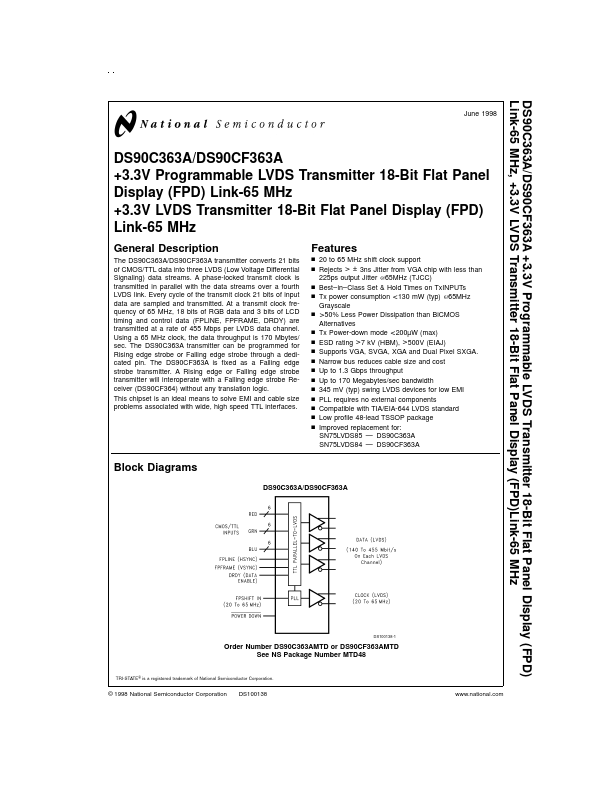
Description
The DS90C363A/DS90CF363A transmitter converts 21 bits of CMOS/TTL data into three LVDS (Low Voltage Differential Signaling) data streams.
A phase-locked transmit clock is transmitted in parallel with the data streams over a fourth LVDS link.
Features
- n 20 to 65 MHz shift clock support n Rejects > ± 3ns Jitter from VGA chip with less than 225ps output Jitter @65MHz (TJCC) n Best.
- in.
- Class Set & Hold Times on TxINPUTs n Tx power consumption < 130 mW (typ) @65MHz Grayscale n > 50% Less Power Dissipation than BiCMOS Alternatives n Tx Power-down mode < 200µW (max) n ESD rating > 7 kV (HBM), > 500V (EIAJ) n Supports VGA, SVGA, XGA and Dual Pixel SXGA. n Narrow bus reduces cable size and cost n Up to 1.3 Gbps throughput n Up to 170 M.
 DS90CF363A Datasheet