Datasheet4U Logo Datasheet4U.com

DM74LS258B - TRI-STATE Quad 2-Data Selectors/Multiplexers

Download the DM74LS258B datasheet PDF. This datasheet also covers the DM74LS257BNationalSemiconductor variant, as both devices belong to the same tri-state quad 2-data selectors/multiplexers family and are provided as variant models within a single manufacturer datasheet.
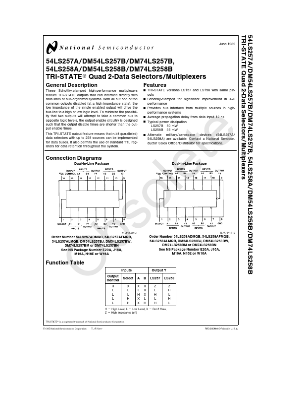
Description

These Schottky-clamped high-performance multiplexers feature TRI-STATE outputs that can interface directly with data lines of bus-organized systems With all but one of the common outputs disabled (at a high impedance state) the low impedance of the single enabled output will drive the bus line to a

Features

  • Y TRI-STATE versions LS157 and LS158 with same pinouts Y Schottky-clamped for significant improvement in A-C performance Y Provides bus interface from multiple sources in highperformance systems Y Average propagation delay from data input 12 ns Y Typical power dissipation LS257B 50 mW LS258B 35 mW Y Alternate military aerospace devices (54LS257A 54LS258A) are available Contact a National Semiconductor Sales Office Distributor for specifications Connection Diagrams Dual-In-Line Package Dual-In-.

📥 Download Datasheet

Note: The manufacturer provides a single datasheet file (DM74LS257BNationalSemiconductor.pdf) that lists specifications for multiple related part numbers.

Full PDF Text Transcription (Reference)

The following content is an automatically extracted verbatim text from the original manufacturer datasheet and is provided for reference purposes only.

View original datasheet text
Obsolete 54LS257A DM54LS257B DM74LS257B 54LS258A DM54LS258B DM74LS258B TRI-STATE Quad 2-Data Selectors Multiplexers June 1989 54LS257A DM54LS257B DM74LS257B 54LS258A DM54LS258B DM74LS258B TRI-STATE Quad 2-Data Selectors Multiplexers General Description These Schottky-clamped high-performance multiplexers feature TRI-STATE outputs that can interface directly with data lines of bus-organized systems With all but one of the common outputs disabled (at a high impedance state) the low impedance of the single enabled output will drive the bus line to a high or low logic level To minimize the possibility that two outputs will attempt to take a common bus to opposite logic levels the output enable circuitry is designed such that the output disable times are shorter than the output enable times
Published: |