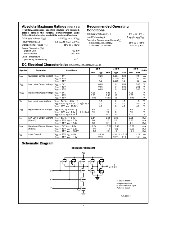
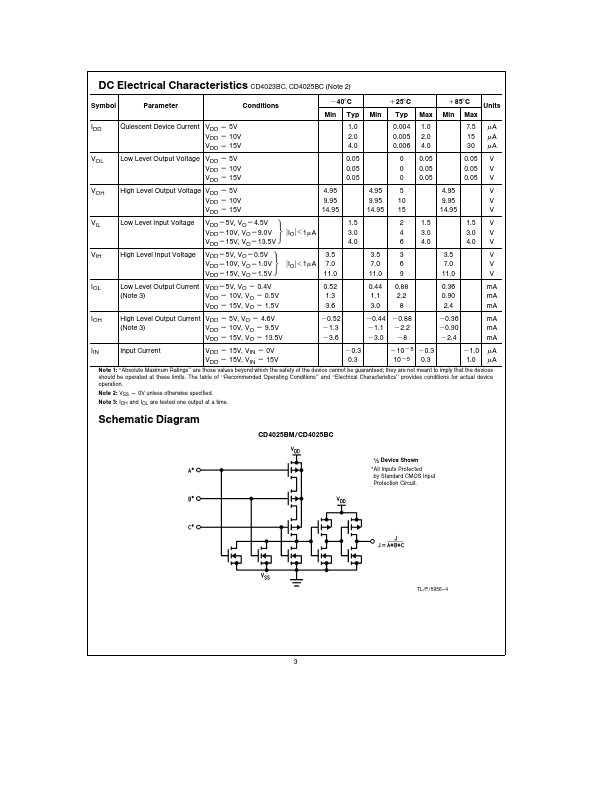
These triple gates are monolithic complementary MOS (CMOS) integrated circuits constructed with N- and P-channel enhancement mode transistors They have equal source and sink current capabilities and conform to standard B series output drive The devices also have buffered outputs which improve transf
Features
Y Y Y
Y Y Y
Wide supply voltage range 3 0V to 15V High noise immunity 0 45 VDD (typ ) Low power TTL fan out of 2 driving 74L compatibility or 1 driving 74LS 5V.
10V.
15V parametric ratings Symmetrical output characteristics Maximum input leakage 1 mA at 15V over full temperature range
Connection Diagrams
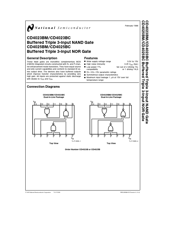
CD4023BM CD4023BC Dual-In-Line Package CD4025BM CD4025BC Dual-In-Line Package
TL F 5956.
1
TL F 5956.
2
Top View Order Number CD4023B or CD4025B
Top Vi.
The following content is an automatically extracted verbatim text
from the original manufacturer datasheet and is provided for reference purposes only.
View original datasheet text
CD4023BM CD4023BC Buffered Triple 3-Input NAND Gate CD4025BM CD4025BC Buffered Triple 3-Input NOR Gate
February 1988
CD4023BM CD4023BC Buffered Triple 3-Input NAND Gate CD4025BM CD4025BC Buffered Triple 3-Input NOR Gate
General Description
These triple gates are monolithic complementary MOS (CMOS) integrated circuits constructed with N- and P-channel enhancement mode transistors They have equal source and sink current capabilities and conform to standard B series output drive The devices also have buffered outputs which improve transfer characteristics by providing very high gain All inputs are protected against static discharge with diodes to VDD and VSS
Features
Y Y Y
Y Y Y
Wide supply voltage range 3 0V to 15V High noise immunity 0 45 VDD (typ ) Low power TTL fan out of 2 driving 7
 CD4023BC Datasheet