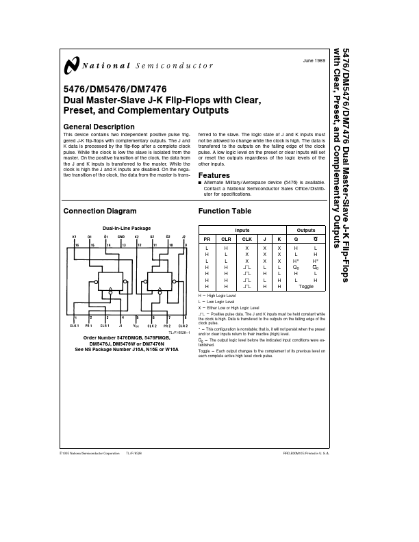
Description
This device contains two independent positive pulse triggered J-K flip-flops with complementary outputs The J and K data is processed by the flip-flop after a complete clock pulse While the clock is low the slave is isolated from the master On the positive transition of the clock the data from the J and K inputs is transferred to the master While the clock is high the J and K inputs are disabled On the negative transition of the clock the data from the master is trans-
ferred to the slave The l
Features
- Y Alternate Military Aerospace device (5476) is available Contact a National Semiconductor Sales Office Distributor for specifications
Connection Diagram
Function Table
Dual-In-Line Package
TL F 6528.
- 1
Order Number 5476DMQB 5476FMQB DM5476J DM5476W or DM7476N
See NS Package Number J16A N16E or W16A
Inputs
Outputs
PR CLR CLK J K
Q
Q
LH HL LL HH HH HH HH
X
XX
H
L
X XX L
H
X
XX
H
H
LL HL
Q0 H
Q0 L
LH
L
H
HH
Toggle
H e High Logic Level
L e Low Logic Level
X e Ei.
 5476-NationalSemiconductor.pdf