Datasheet4U Logo Datasheet4U.com

AQ2A2-C2-T5VDC - SOLID STATE RELAY

Download the AQ2A2-C2-T5VDC datasheet PDF. This datasheet also covers the AQ2A1-C1-ZT5VDC variant, as both devices belong to the same solid state relay family and are provided as variant models within a single manufacturer datasheet.
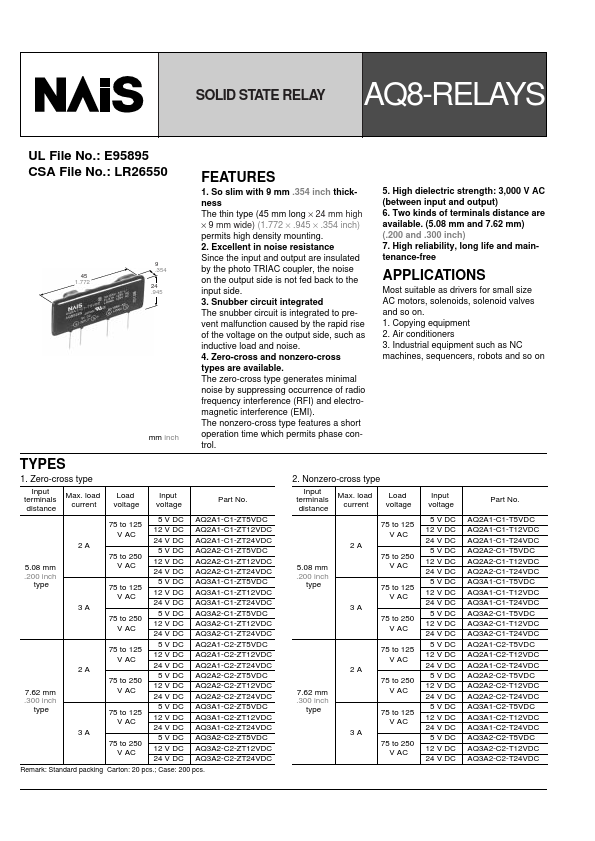
Features

  • 1. So slim with 9 mm .354 inch thickness The thin type (45 mm long × 24 mm high × 9 mm wide) (1.772 × .945 × .354 inch) permits high density mounting. 2. Excellent in noise resistance Since the input and output are insulated by the photo TRIAC coupler, the noise on the output side is not fed back to the input side. 3. Snubber circuit integrated The snubber circuit is integrated to prevent malfunction caused by the rapid rise of the voltage on the output side, such as inductive load and noise. 4.

📥 Download Datasheet

Note: The manufacturer provides a single datasheet file (AQ2A1-C1-ZT5VDC-Nais.pdf) that lists specifications for multiple related part numbers.

Datasheet Details

Part number AQ2A2-C2-T5VDC
Manufacturer Nais
File Size 157.20 KB
Description SOLID STATE RELAY
Datasheet download datasheet AQ2A2-C2-T5VDC Datasheet

Full PDF Text Transcription (Reference)

The following content is an automatically extracted verbatim text from the original manufacturer datasheet and is provided for reference purposes only.

View original datasheet text
SOLID STATE RELAY AQ8-RELAYS 5. High dielectric strength: 3,000 V AC (between input and output) 6. Two kinds of terminals distance are available. (5.08 mm and 7.62 mm) (.200 and .300 inch) 7. High reliability, long life and maintenance-free UL File No.: E95895 CSA File No.: LR26550 FEATURES 1. So slim with 9 mm .354 inch thickness The thin type (45 mm long × 24 mm high × 9 mm wide) (1.772 × .945 × .354 inch) permits high density mounting. 2. Excellent in noise resistance Since the input and output are insulated by the photo TRIAC coupler, the noise on the output side is not fed back to the input side. 3. Snubber circuit integrated The snubber circuit is integrated to prevent malfunction caused by the rapid rise of the voltage on the output side, such as inductive load and noise. 4.
Published: |