Datasheet Details
| Part number | LPC832 |
|---|---|
| Manufacturer | NXP Semiconductors |
| File Size | 1.75 MB |
| Description | 32-bit ARM Cortex-M0+ microcontroller |
| Datasheet |
 LPC832 Datasheet LPC832 Datasheet
|
|
|
This page provides the datasheet information for the LPC832, a member of the LPC834 32-bit ARM Cortex-M0+ microcontroller family.
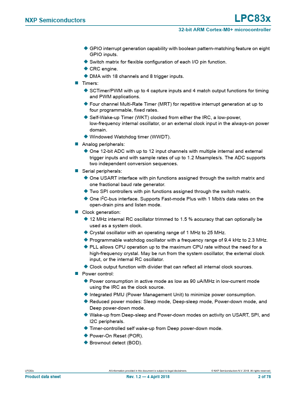
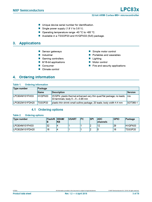
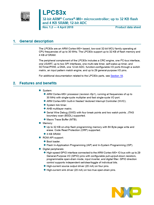
The LPC83x are an ARM Cortex-M0+ based, low-cost 32-bit MCU family operating at CPU frequencies of up to 30 MHz.
The LPC83x support up to 32 KB of flash memory and 4 KB of SRAM.
| Part number | LPC832 |
|---|---|
| Manufacturer | NXP Semiconductors |
| File Size | 1.75 MB |
| Description | 32-bit ARM Cortex-M0+ microcontroller |
| Datasheet |
LPC832 Datasheet
|
|
|
|