The following content is an automatically extracted verbatim text
from the original manufacturer datasheet and is provided for reference purposes only.
View original datasheet text
Technical Data
2N2609 JAN POWER MOSFET P CHANNEL
Processed per MIL-PRF-19500/296
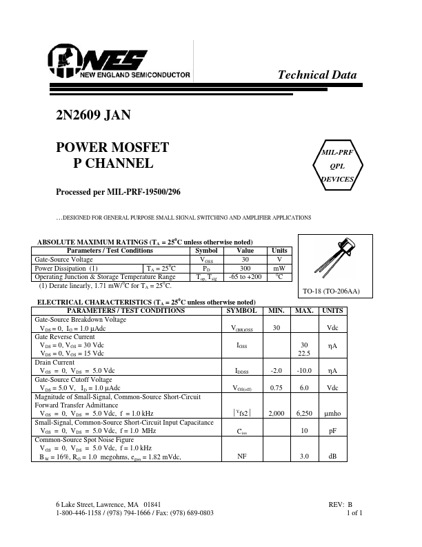
…DESIGNED FOR GENERAL PURPOSE SMALL SIGNAL SWITCHING AND AMPLIFIER APPLICATIONS ABSOLUTE MAXIMUM RATINGS (TA = 250C unless otherwise noted) Parameters / Test Conditions Symbol Value Gate-Source Voltage VGSS 30 0 Power Dissipation (1) TA = 25 C PD 300 Operating Junction & Storage Temperature Range Top, Tstg -65 to +200 (1) Derate linearly, 1.71 mW/ 0C for TA = 250C. ELECTRICAL CHARACTERISTICS (TA = 25 C unless otherwise noted) PARAMETERS / TEST CONDITIONS SYMBOL Gate-Source Breakdown Voltage V(BR)GSS V DS = 0, IG = 1.0 µAdc Gate Reverse Current V DS = 0, VGS = 30 Vdc IGSS VDS = 0, VGS = 15 Vdc Drain Current V GS = 0, V DS = 5.0 Vdc IDDSS Gate-Source Cutoff Voltage VGS(off) V DS = 5.0 V, I D = 1.
 2N2609 Datasheet