Datasheet4U Logo Datasheet4U.com

MPC950 - (MPC950 / MPC951) LOW VOLTAGE PLL CLOCK DRIVER

Download the MPC950 datasheet PDF. This datasheet also covers the MPC951 variant, as both devices belong to the same (mpc950 / mpc951) low voltage pll clock driver family and are provided as variant models within a single manufacturer datasheet.

Features

  • allow for the MPC951 to be used as a zero delay, low skew fanout buffer. In addition, the external feedback allows for a wider variety of input.
  • to.
  • output frequency relationships. The MPC951 REF_SEL pin allows for the selection of an alternate LVCMOS input clock to be used as a test clock or to provide the reference for the PLL from an LVCMOS source. The MPC950 provides an external test clock input for scan clock distribution or system diagnostics. In addition the REF_SEL pin allo.

📥 Download Datasheet

Note: The manufacturer provides a single datasheet file (MPC951_Motorola.pdf) that lists specifications for multiple related part numbers.

Full PDF Text Transcription

Click to expand full text
MOTOROLA SEMICONDUCTOR TECHNICAL DATA 
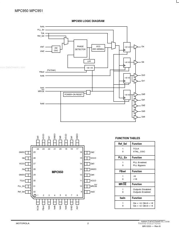
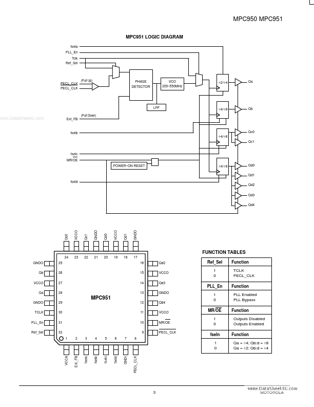
Low Voltage PLL Clock Driver The MPC950/951 are 3.3V compatible, PLL based clock driver devices targeted for high performance clock tree designs. With output frequencies of up to 180MHz and output skews of 375ps the MPC950 is ideal for the most demanding clock tree designs. The devices employ a fully differential PLL design to minimize cycle–to–cycle and long term jitter. This parameter is of significant importance when the clock driver is providing the reference clock for PLL’s on board today’s microprocessors and ASiC’s. The devices offer 9 low skew outputs, the outputs are configurable to support the clocking needs of the various high performance microprocessors. www.DataSheet4U.
Published: |