The following content is an automatically extracted verbatim text
from the original manufacturer datasheet and is provided for reference purposes only.
View original datasheet text
MOTOROLA
SEMICONDUCTOR TECHNICAL DATA
Order this document by MCM36F8/D
Advance Information
1MB and 2MB Synchronous Fast Static RAM Module
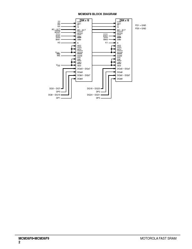
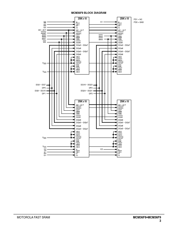
The MCM36F8 (1MB) is configured as 256K x 36 bits and the MCM36F9 (2MB) is configured as 512K x 36 bits. Both are packaged in a 144–pin dual–in–line memory module (DIMM). Each module uses Motorola’s 3.3 V 256K x 18 bit flow– through BurstRAMs. Address (A), data inputs (DQ, DP), and all control signals except output enable (G) are clock (K) controlled through positive–edge–triggered noninverting registers. Write cycles are internally self–timed and initiated by the rising edge of the clock (K) input. This feature provides increased timing flexibility for incoming signals.
 MCM36F9 Datasheet