Click to expand full text
MOTOROLA
SEMICONDUCTOR TECHNICAL DATA
Order this document by BSS123LT1/D
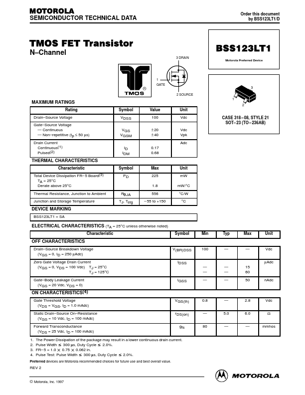
TMOS FET Transistor
N–Channel
3 DRAIN 1 GATE 2 SOURCE
BSS123LT1
Motorola Preferred Device
®
MAXIMUM RATINGS
Rating Drain–Source Voltage Gate–Source Voltage — Continuous — Non–repetitive (tp ≤ 50 µs) Drain Current Continuous(1) Pulsed(2) Symbol VDSS VGS VGSM ID IDM
3 1 2
Value 100 ± 20 ± 40 0.17 0.68
Unit Vdc Vdc Vpk Adc CASE 318 – 08, STYLE 21 SOT– 23 (TO – 236AB)
THERMAL CHARACTERISTICS
Characteristic Total Device Dissipation FR– 5 Board(3) TA = 25°C Derate above 25°C Thermal Resistance, Junction to Ambient Junction and Storage Temperature Symbol PD Max 225 1.
 BSS123LT1 Datasheet