Datasheet Details
| Part number | M2V64S40BTP-8L |
|---|---|
| Manufacturer | Mitsubishi Electric |
| File Size | 741.74 KB |
| Description | 64M bit Synchronous DRAM |
| Datasheet |
 M2V64S40BTP-8L Datasheet M2V64S40BTP-8L Datasheet
|
|
|
This page provides the datasheet information for the M2V64S40BTP-8L, a member of the M2V64S20BTP-7 64M bit Synchronous DRAM family.
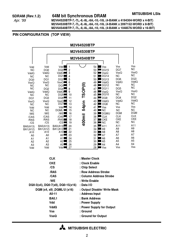
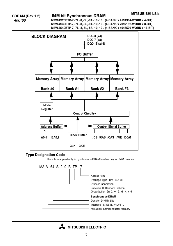
The M2V64S20BTP is organized as 4-bank x 4194304-word x 4-bit, M2V64S30BTP is organized as 4-bank x 2097152-word x 8-bit, and M2V64S40BTP is organized as 4-bank x 1048576-word x 16-bit Synchronous DRAM with LVTTL interface.
All inputs and outputs are referenced to the rising edge of CLK.
| Part number | M2V64S40BTP-8L |
|---|---|
| Manufacturer | Mitsubishi Electric |
| File Size | 741.74 KB |
| Description | 64M bit Synchronous DRAM |
| Datasheet |
M2V64S40BTP-8L Datasheet
|
|
|
|