Datasheet Details
| Part number | M2V28S30ATP |
|---|---|
| Manufacturer | Mitsubishi Electric |
| File Size | 626.92 KB |
| Description | 128M Synchronous DRAM |
| Datasheet |
 M2V28S30ATP Datasheet M2V28S30ATP Datasheet
|
|
|
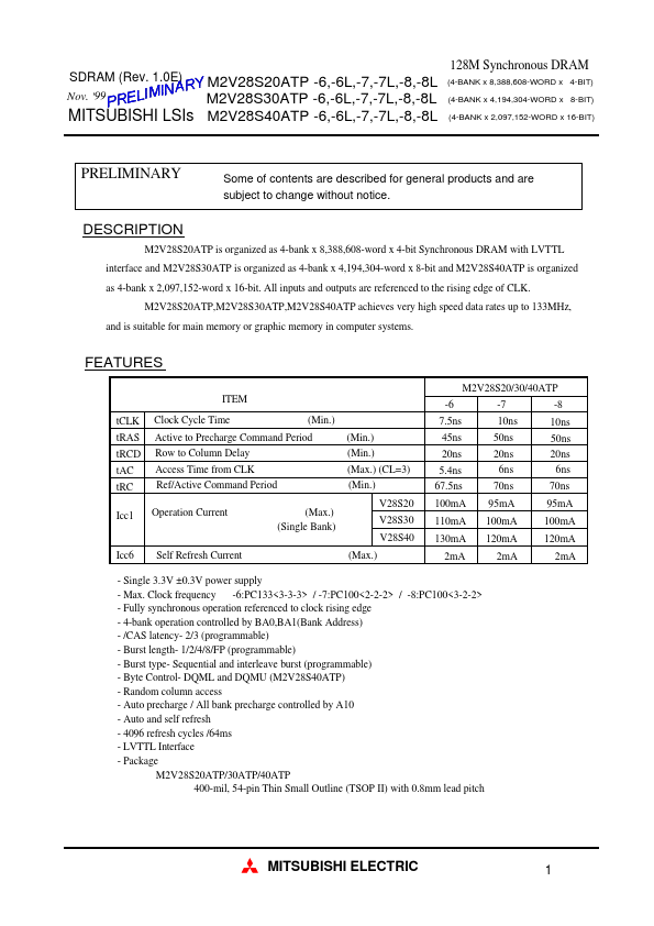
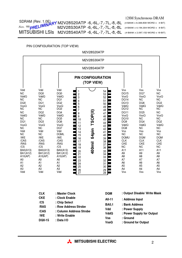
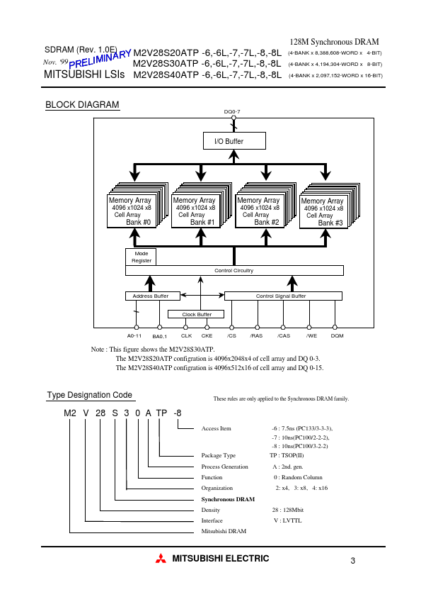
M2V28S20ATP is organized as 4-bank x 8,388,608-word x 4-bit Synchronous DRAM with LVTTL interface and M2V28S30ATP is organized as 4-bank x 4,194,304-word x 8-bit and M2V28S40ATP is organized as 4-bank x 2,097,152-word x 16-bit.
All inputs and outputs are referenced to the rising edge of CLK.
| Part number | M2V28S30ATP |
|---|---|
| Manufacturer | Mitsubishi Electric |
| File Size | 626.92 KB |
| Description | 128M Synchronous DRAM |
| Datasheet |
M2V28S30ATP Datasheet
|
|
|
|