Datasheet Details
| Part number | CGB7015-BD |
|---|---|
| Manufacturer | Mimix Broadband |
| File Size | 224.35 KB |
| Description | MMIC or Packaged Matched Gain Block Amplifier |
| Datasheet |
 CGB7015-BD Datasheet CGB7015-BD Datasheet
|
|
|
Download the CGB7015-BD datasheet PDF. This datasheet also covers the CGB7015-SC variant, as both devices belong to the same mmic or packaged matched gain block amplifier family and are provided as variant models within a single manufacturer datasheet.
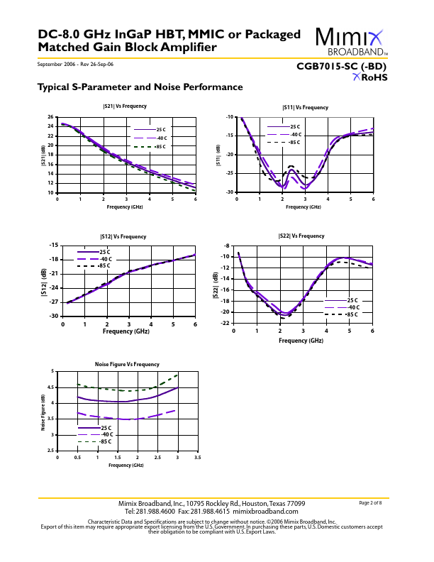
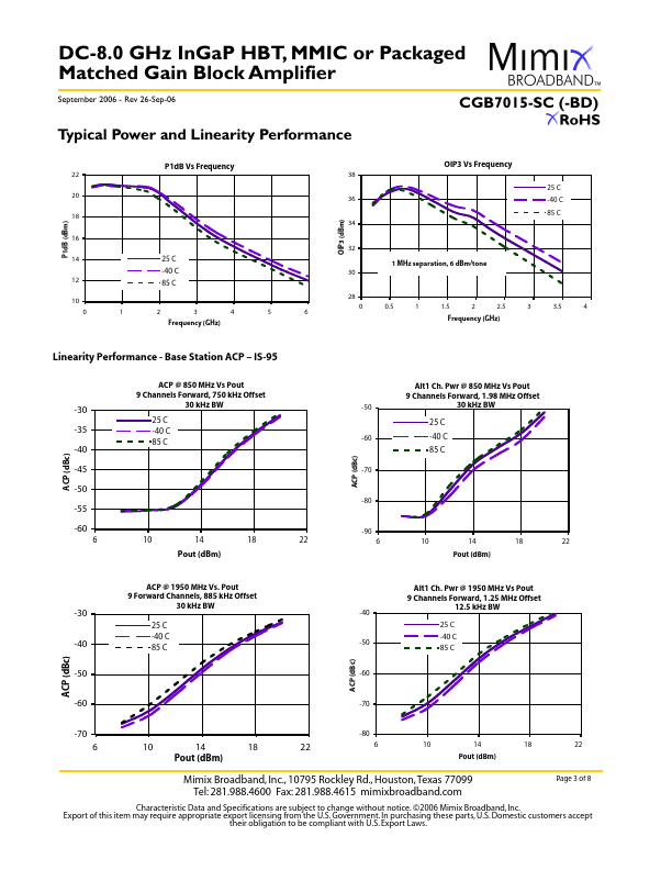
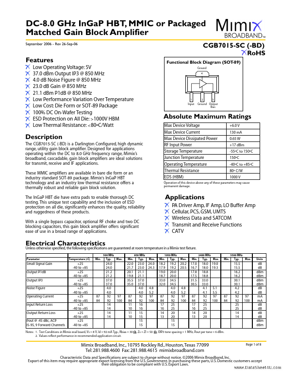
The CGB7015-SC (-BD) is a Darlington Configured, high dynamic range, utility gain block amplifier.
Designed for applications operating within the DC to 8.0 GHz frequency range, Mimix’s broadband, cascadable, gain block amplifiers are ideal solutions for transmit, receive and IF applications.
| Part number | CGB7015-BD |
|---|---|
| Manufacturer | Mimix Broadband |
| File Size | 224.35 KB |
| Description | MMIC or Packaged Matched Gain Block Amplifier |
| Datasheet |
CGB7015-BD Datasheet
|
|
|
|
| Part Number | Description | Manufacturer |
|---|---|---|
| CGB-1089Z | Single Ended InGaP/GaAs HBT MMIC CATV Amplifier | Sirenza Microdevices |
| CGB240 | 2-Stage Bluetooth InGaP HBT Power Amplifier | TriQuint Semiconductor |
| CGB240B | 2-Stage Bluetooth & WLAN InGaP HBT Power Amplifier | TriQuint Semiconductor |
| CGB241 | 2-Stage Bluetooth & WLAN InGaP HBT Power Amplifier | TriQuint Semiconductor |
| Part Number | Description |
|---|---|
| CGB7015-SC | MMIC or Packaged Matched Gain Block Amplifier |
| CGB7010-BD | MMIC or Packaged Matched Gain Block Amplifier |
| CGB7010-SC | MMIC or Packaged Matched Gain Block Amplifier |
| CGB7011-BD | MMIC or Packaged Matched Gain Block Amplifier |
| CGB7011-SC | MMIC or Packaged Matched Gain Block Amplifier |
The following content is an automatically extracted verbatim text from the original manufacturer datasheet and is provided for reference purposes only.