Datasheet Details
- Part number
- MX23L6410MC-12, MX23L6410
- Manufacturer
- Macronix International
- File Size
- 715.39 KB
- Datasheet
- MX23L6410_MacronixInternational.pdf
- Description
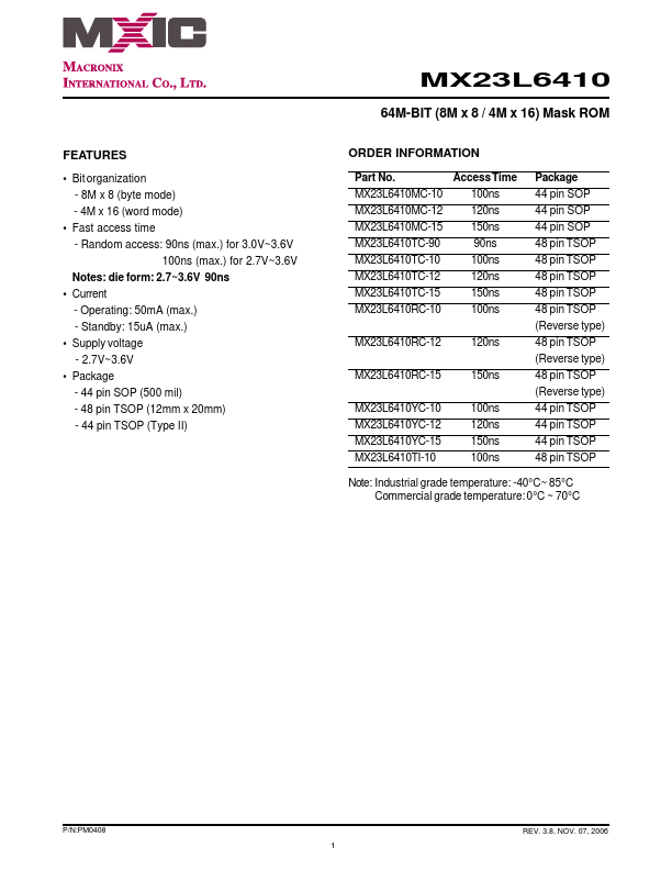
- 64M-BIT (8M x 8 / 4M x 16) Mask ROM
- Note
- This datasheet PDF includes multiple part numbers: MX23L6410MC-12, MX23L6410.
Please refer to the document for exact specifications by model.