Datasheet Details
| Part number | LTC6957-1 |
|---|---|
| Manufacturer | Linear Technology (now Analog Devices) |
| File Size | 1.37 MB |
| Description | Dual Output Buffer/Driver/Logic Converter |
| Datasheet |
 LTC6957-1 Datasheet LTC6957-1 Datasheet
|
|
|
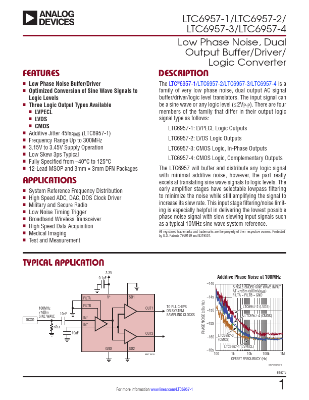
The LTC®6957-1/LTC6957-2/LTC6957-3/LTC6957-4 is a family of very low phase noise, dual output AC signal buffer/driver/logic level translators.
The input signal can be a sine wave or any logic level (≤2VP-P).
| Part number | LTC6957-1 |
|---|---|
| Manufacturer | Linear Technology (now Analog Devices) |
| File Size | 1.37 MB |
| Description | Dual Output Buffer/Driver/Logic Converter |
| Datasheet |
LTC6957-1 Datasheet
|
|
|
|