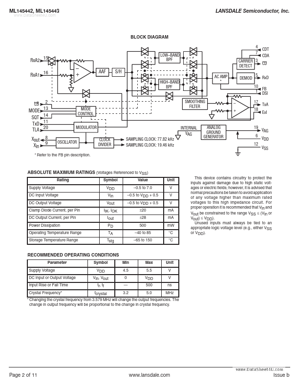
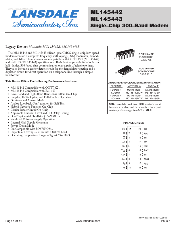
Description
ABSOLUTE MAXIMUM RATINGS (Voltages Referenced to VSS)
Rating Supply Voltage DC Input Voltage DC Output Voltage Clamp Diode Current, per Pin DC Output Current, per Pin Power Dissipation Operating Temperature Range Storage Temperature Range Symbol VDD Vin Vout IIK, IOK Iout PD TA Tstg Value
0.5 to 7.0
0.5 to VDD + 0.5
0.5 to VDD + 0.5 ±20 ±28 500
40 to 85
65 to 150 Unit V V V mA mA mW °C °C This device contains circuitry to protect the inputs against
Features
- ML145442 Compatible with CCITT V .21 ML145443 Compatible with Bell 103 Low.
- Band and High.
- Band Band.
- Pass Filters On.
- Chip Simplex, Half.
- Duplex, and Full.
- Duplex Operation Originate and Answer Mode Analog Loopback Configuration for Self Test Hybrid Network Function On.
- Chip Carrier Detec.
 ML145442_LANSDALESemiconductor.pdf