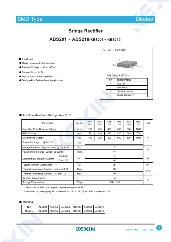
PIN DESCRIPTION 1 Input Pin (~) 2 Input Pin (~) 3 Output Anode (+) 4 Output Cathode (-)
Ƶ Absolute Maximum Ratings Ta = 25ć
Parameter
Repetitive Peak Reverse Voltage RMS Voltage DC Blocking Voltage Forward Voltage @ IF=2A
Average Rectified Output Current @ Tc= 115ć
Peak Forward Surge Current @
Features
ƽ Glass Passivated Chip Junction ƽ Reverse Voltage - 100 to 1000 V
ƽ Forward Current - 2A ƽ High Surge Current Capability ƽ Designed for Surface Mount.
The following content is an automatically extracted verbatim text
from the original manufacturer datasheet and is provided for reference purposes only.
View original datasheet text
SMD Type
TransDisiotodress
Bridge Rectifier ABS201 ~ ABS210(KBS201 ~ KBS210)
Ƶ Features
ƽ Glass Passivated Chip Junction ƽ Reverse Voltage - 100 to 1000 V
ƽ Forward Current - 2A ƽ High Surge Current Capability ƽ Designed for Surface Mount Application
ABS/LBF Package
3 4
2 1
PIN DESCRIPTION
PIN DESCRIPTION 1 Input Pin (~) 2 Input Pin (~) 3 Output Anode (+) 4 Output Cathode (-)
Ƶ Absolute Maximum Ratings Ta = 25ć
Parameter
Repetitive Peak Reverse Voltage RMS Voltage DC Blocking Voltage Forward Voltage @ IF=2A
Average Rectified Output Current @ Tc= 115ć
Peak Forward Surge Current @ 8.3ms
Maximum DC Reverse Current
Ta=25ć Ta=125ć
Typical Junction Capacitance *1
Thermal Resistance.Junction- to-Ambient *2
Thermal Resistance.
 ABS201 Datasheet