The following content is an automatically extracted verbatim text
from the original manufacturer datasheet and is provided for reference purposes only.
View original datasheet text
TECHNICAL DATA
www.DataSheet4U.com
KK7407
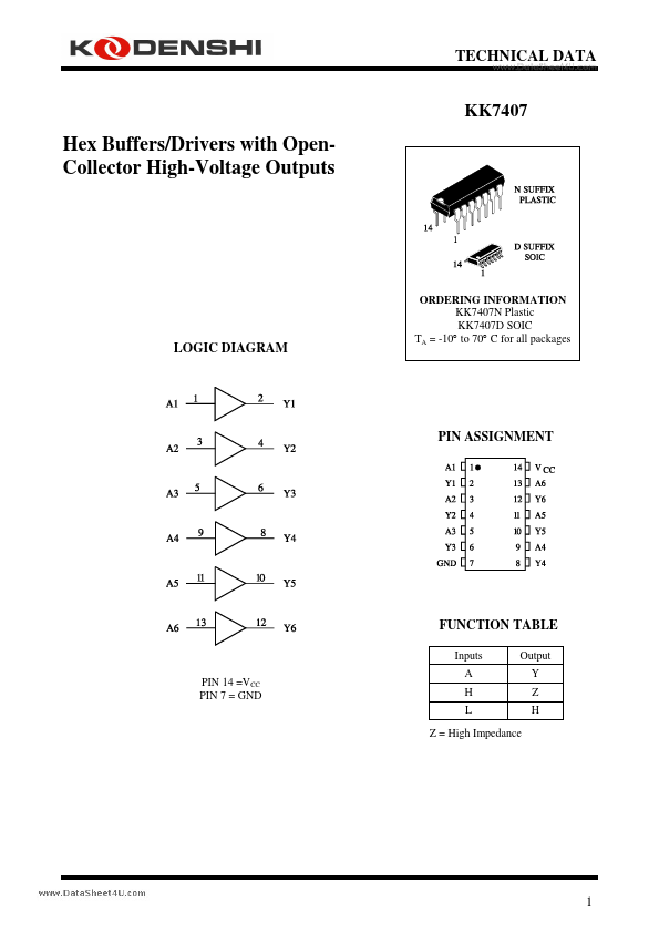
Hex Buffers/Drivers with OpenCollector High-Voltage Outputs
LOGIC DIAGRAM
ORDERING INFORMATION KK7407N Plastic KK7407D SOIC TA = -10° to 70° C for all packages
PIN ASSIGNMENT
FUNCTION TABLE
Inputs PIN 14 =VCC PIN 7 = GND A H L Z = High Impedance Output Y Z H
1
www.DataSheet4U.com
KK7407
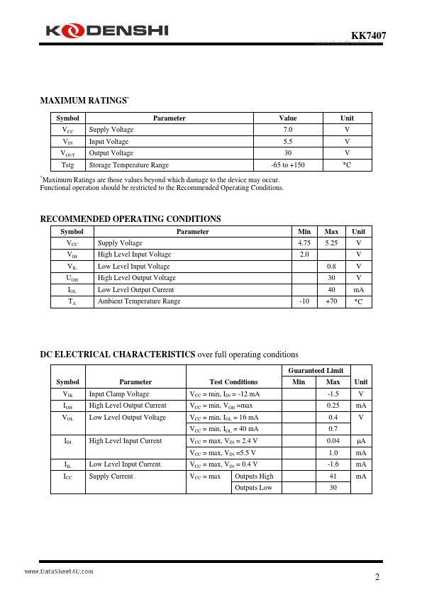
MAXIMUM RATINGS*
Symbol VCC VIN VOUT Tstg
*
Parameter Supply Voltage Input Voltage Output Voltage Storage Temperature Range
Value 7.0 5.5 30 -65 to +150
Unit V V V °C
Maximum Ratings are those values beyond which damage to the device may occur. Functional operation should be restricted to the Recommended Operating Conditions.
 KK7407 Datasheet