The following content is an automatically extracted verbatim text
from the original manufacturer datasheet and is provided for reference purposes only.
View original datasheet text
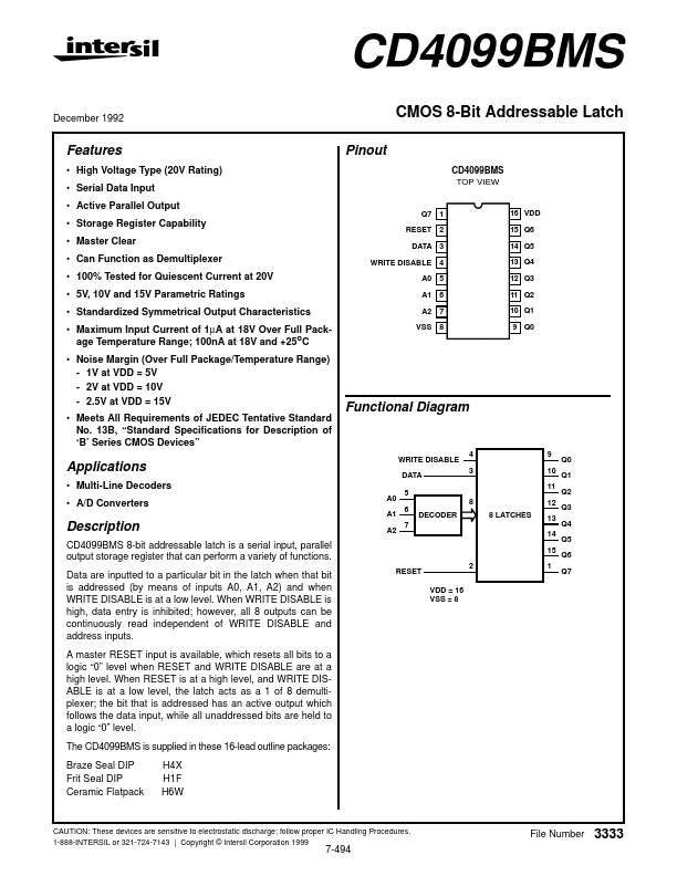
CD4099BMS
December 1992
CMOS 8-Bit Addressable Latch
Pinout
CD4099BMS TOP VIEW
Features
• High Voltage Type (20V Rating) • Serial Data Input • Active Parallel Output
Q7
1 2
16 VDD 15 Q6 14 Q5 13 Q4 12 Q3 11 Q2 10 Q1 9 Q0
• Storage Register Capability • Master Clear • Can Function as Demultiplexer • 100% Tested for Quiescent Current at 20V • 5V, 10V and 15V Parametric Ratings • Standardized Symmetrical Output Characteristics • Maximum Input Current of 1µA at 18V Over Full Package Temperature Range; 100nA at 18V and +25oC • Noise Margin (Over Full Package/Temperature Range) - 1V at VDD = 5V - 2V at VDD = 10V - 2.5V at VDD = 15V • Meets All Requirements of JEDEC Tentative Standard No.
 CD4099BMS Datasheet