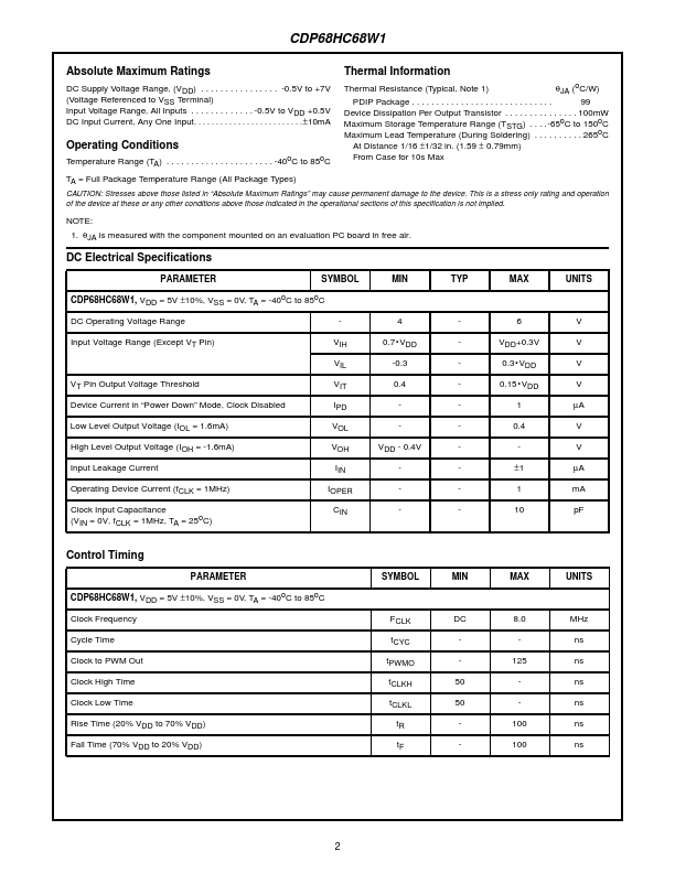
Datasheet4U Logo Datasheet4U.com

68HC68W1 - CMOS Serial Digital Pulse Width Modulator

Description

The CDP68HC68W1 modulates a clock input to supply a variable frequency and duty-cycle output signal.

Three 8-bit registers (pulse width, frequency and control) are accessed serially after power is applied to initialize device operation.

Features

  • Programmable Frequency and Duty Cycle Output.
  • Serial Bus Input; Compatible with Motorola/Intersil SPI Bus, Simple Shift-Register Type Interface.
  • 8 Lead PDIP Package.
  • Schmitt Trigger Clock Input.
  • 4V to 6V Operation, -40oC to 85oC Temperature Range.
  • 8MHz Clock Input Frequency
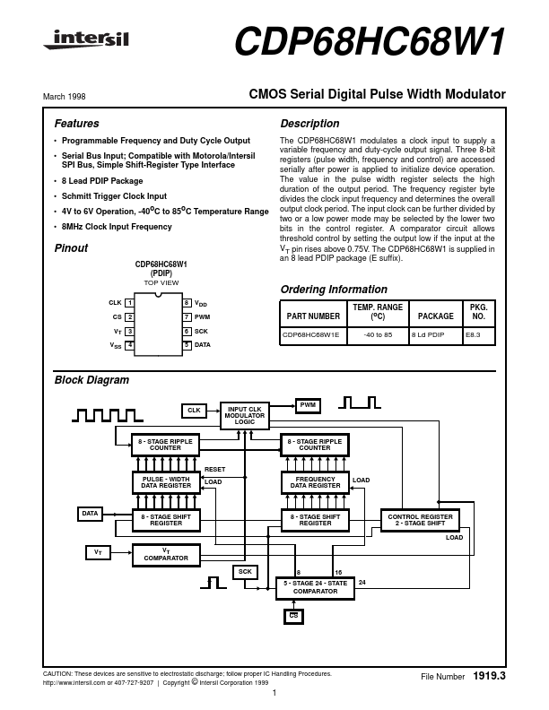
 Pinout CDP68HC68W1 (PDIP) TOP VIEW CLK CS VT VSS 1 2 3 4 8 7 6 5 VDD PWM SCK DATA Ordering Information PART NUMBER CDP68HC68W1E TEMP. RANGE (oC) -40 to 85.

📥 Download Datasheet

Full PDF Text Transcription (Reference)

The following content is an automatically extracted verbatim text from the original manufacturer datasheet and is provided for reference purposes only.

View original datasheet text
CDP68HC68W1 March 1998 CMOS Serial Digital Pulse Width Modulator Description The CDP68HC68W1 modulates a clock input to supply a variable frequency and duty-cycle output signal. Three 8-bit registers (pulse width, frequency and control) are accessed serially after power is applied to initialize device operation. The value in the pulse width register selects the high duration of the output period. The frequency register byte divides the clock input frequency and determines the overall output clock period. The input clock can be further divided by two or a low power mode may be selected by the lower two bits in the control register. A comparator circuit allows threshold control by setting the output low if the input at the VT pin rises above 0.75V.
Published: |