The following content is an automatically extracted verbatim text
from the original manufacturer datasheet and is provided for reference purposes only.
View original datasheet text
PD -96203
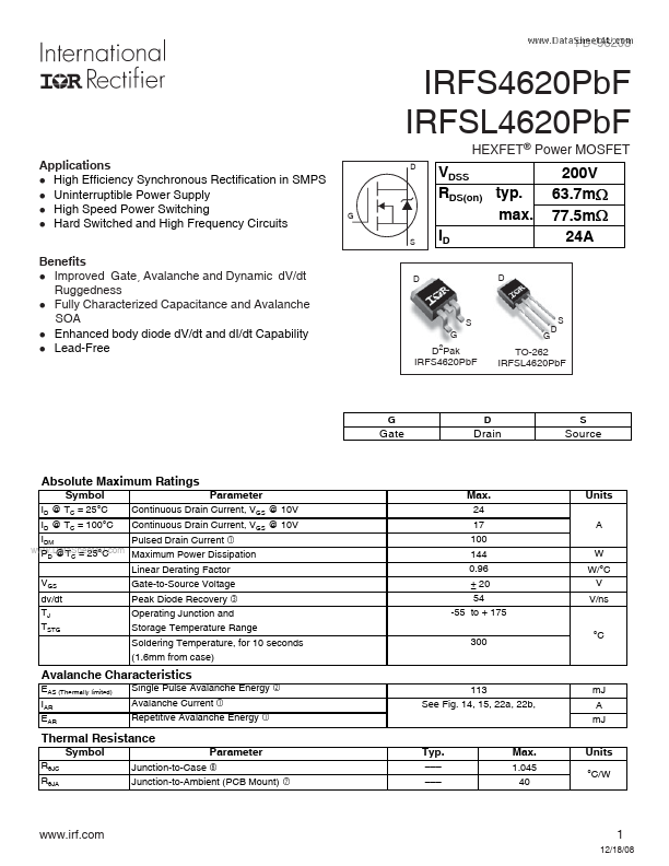
IRFS4620PbF IRFSL4620PbF
HEXFET® Power MOSFET
Applications l High Efficiency Synchronous Rectification in SMPS l Uninterruptible Power Supply l High Speed Power Switching l Hard Switched and High Frequency Circuits Benefits l Improved Gate, Avalanche and Dynamic dV/dt Ruggedness l Fully Characterized Capacitance and Avalanche SOA l Enhanced body diode dV/dt and dI/dt Capability l Lead-Free
D G S
VDSS RDS(on) typ. max. ID
D
200V 63.7m: 77.5m: 24A
D
S G G
D
S
D2Pak IRFS4620PbF
TO-262 IRFSL4620PbF
G
D
S
Gate
Drain
Source
Absolute Maximum Ratings
Symbol
ID @ TC = 25°C
Parameter
Continuous Drain Current, VGS @ 10V Continuous Drain Current, VGS @ 10V
Max.
24 17 100 144 0.96 ± 20 54 -55 to + 175 300
Units
A W W/°C V V/ns
ID @ TC = 100°C IDM Pulsed Drain Current www.
 IRFS4620PBF Datasheet