Datasheet Details
| Part number | ICS9LP525-2 |
|---|---|
| Manufacturer | Integrated Device Technology |
| File Size | 269.62 KB |
| Description | 56-pin CK505 Clock |
| Datasheet |
 ICS9LP525-2_IntegratedDeviceTechnology.pdf ICS9LP525-2_IntegratedDeviceTechnology.pdf
|
| Part number | ICS9LP525-2 |
|---|---|
| Manufacturer | Integrated Device Technology |
| File Size | 269.62 KB |
| Description | 56-pin CK505 Clock |
| Datasheet |
ICS9LP525-2_IntegratedDeviceTechnology.pdf
|
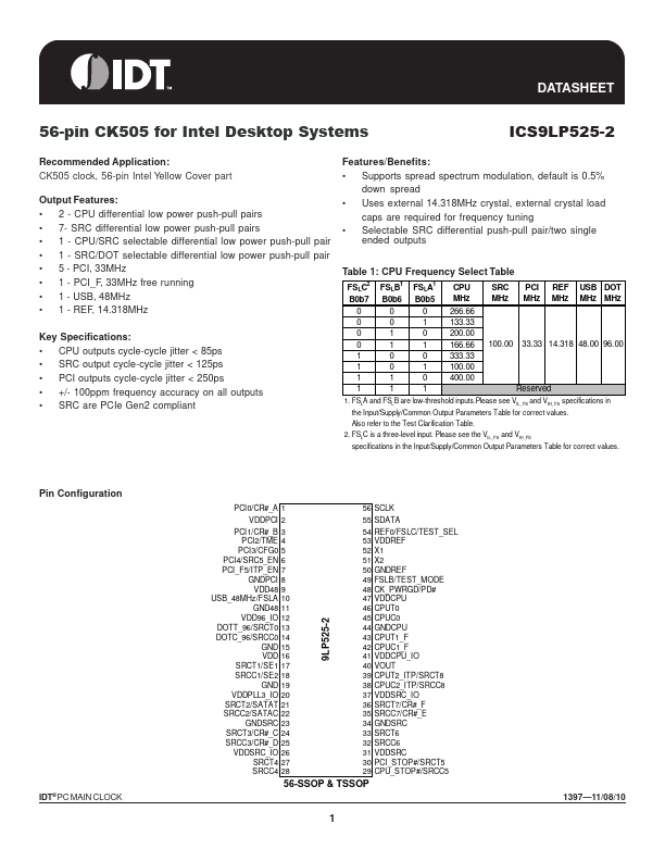
PIN # PIN NAME TYPE DESCRIPTION 3.3V PCI clock output or Clock Request control A for either SRC0 or SRC2 pair The power-up default is PCI0 output, but this pin may also be used as a Clock Request control of SRC pair 0 or SRC pair 2 via SMBus.Before configuring this pin as a Clock Request Pin, the PCI output must first be disabled in byte 2, bit 0 of SMBus address space .After the PCI output is disabled (high-Z), the pin can then be set to serve as a Clock Request pin for either SRC pair 2 or p
📁 ICS9LP525-2 Similar Datasheet