Datasheet Details
| Part number | ICS8312 |
|---|---|
| Manufacturer | Integrated Device Technology |
| File Size | 1.08 MB |
| Description | 1-TO-12 LVCMOS/LVTTL FANOUT BUFFER |
| Datasheet |
 ICS8312 Datasheet ICS8312 Datasheet
|
|
|
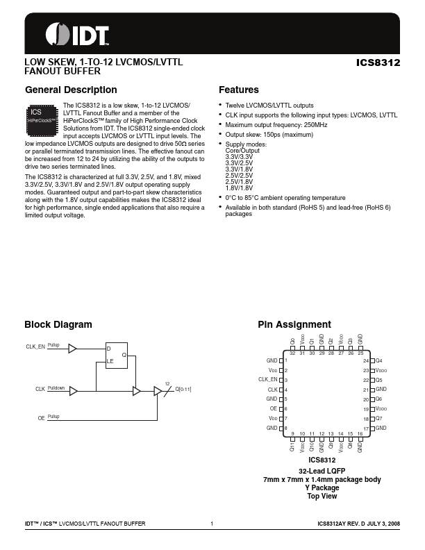
Solutions from IDT.
The ICS8312 single-ended clock input accepts LVCMOS or LVTTL input levels.
| Part number | ICS8312 |
|---|---|
| Manufacturer | Integrated Device Technology |
| File Size | 1.08 MB |
| Description | 1-TO-12 LVCMOS/LVTTL FANOUT BUFFER |
| Datasheet |
ICS8312 Datasheet
|
|
|
|